PI3C3126QE Pericom Semiconductor, PI3C3126QE Datasheet - Page 2
PI3C3126QE
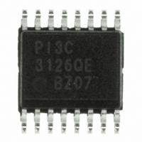
Manufacturer Part Number
PI3C3126QE
Description
IC 4-BIT BUS SW 2-PORT 16-QSOP
Manufacturer
Pericom Semiconductor
Type
FET Bus Switchr
Datasheet
1.PI3C3126QE.pdf
(7 pages)
Specifications of PI3C3126QE
Circuit
4 x 1:1
Voltage Supply Source
Single Supply
Voltage - Supply
3 V ~ 3.6 V
Mounting Type
Surface Mount
Package / Case
16-QSOP
Number Of Switches
Quad
Propagation Delay Time
0.25 ns at 2.5 V to 3.3 V
Supply Voltage (max)
3.63 V
Maximum Operating Temperature
+ 85 C
Minimum Operating Temperature
- 40 C
Mounting Style
SMD/SMT
On Resistance (max)
8 Ohms
Number Of Bits
4
Number Of Elements
4
Technology
CMOS
High Level Output Current
-120mA
Low Level Output Current
120mA
On Resistance
8Ohm
Package Type
QSOP
Operating Temp Range
-40C to 85C
Operating Temperature Classification
Industrial
Operating Supply Voltage (typ)
2.5/3.3V
Operating Supply Voltage (max)
3.63V
Quiescent Current
500uA
Pin Count
16
Mounting
Surface Mount
Lead Free Status / RoHS Status
Lead free / RoHS Compliant
Operating Temperature
-
Current - Output High, Low
-
Independent Circuits
-
Lead Free Status / Rohs Status
Lead free / RoHS Compliant
Available stocks
Company
Part Number
Manufacturer
Quantity
Price

Part Number:
PI3C3126QE
Manufacturer:
PERICOM
Quantity:
20 000


Pin Description
Maximum Ratings
(Above which the useful life may be impaired. For user guidelines, not tested.)
14-Pin Confi gurations
Storage Temperature ............................................................ –65°C to +150°C
Ambient Temperature with Power Applied ........................... –40°C to +85°C
Supply Voltage to Ground Potential (Inputs & V
Supply Voltage to Ground Potential (Outputs & D/O Only) ..–0.5V to +4.6V
DC Input Voltage .................................................................... –0.5V to +5.5V
DC Output Current ............................................................................... 120mA
Power Dissipation ................................................................................... 0.5W
Pin Name
A3 - A0
B3 - B0
GND
09-0075
BEn
V
CC
GND
BE0
BE1
A0
B0
A1
B1
1
2
3
4
5
6
7
14-PIN
Switch Enable
Description
Ground
Power
Bus A
Bus B
14
13
12
11
10
9
8
Vcc
BE3
A3
B3
BE2
A2
B2
CC
Only) .....–0.5V to +4.6V
2
16-Pin Confi gurations
Truth Table
Note:
1. H = High Voltage Level, L = Low Voltage Level
HI-Z = High Impedance, X = Don’t Care
* A pull-up resistor should be provided for power-up protection.
2.5V/3.3V, High Bandwidth, Hot Insertion,4-Bit,
BEn
X*
H
L
2-Port Bus Switch with Individual Enables
Note:
Stresses greater than those listed under MAXIMUM
RATINGS may cause permanent damage to the
device. This is a stress rating only and functional
operation of the device at these or any other
conditions above those indicated in the operational
sections of this specifi cation is not implied. Exposure
to absolute maximum rating conditions for extended
periods may affect reliability.
GND
BE0
BE1
(1)
NC
A0
B0
A1
B1
Hi-Z
Hi-Z
An
Bn
1
2
3
4
5
6
7
8
Hi-Z
Hi-Z
Bn
An
16-PIN
GND
V
V
V
CC
CC
CC
16
15
14
13
12
11
10
9
PS8344
Disconnect
Disconnect
Disconnect
Function
Vcc
BE3
A3
B3
BE2
A2
B2
NC
PI3C3125
11/04/09
Related parts for PI3C3126QE
Image
Part Number
Description
Manufacturer
Datasheet
Request
R

Part Number:
Description:
Fast CMOS bus interface register
Manufacturer:
Pericom Semiconductor
Datasheet:
Part Number:
Description:
4-bit,4-port bus exchange switch
Manufacturer:
Pericom Semiconductor
Datasheet:
Part Number:
Description:
Manufacturer:
Pericom Semiconductor
Datasheet:
Part Number:
Description:
Manufacturer:
Pericom Semiconductor
Datasheet:
Part Number:
Description:
Manufacturer:
Pericom Semiconductor
Datasheet:
Part Number:
Description:
Manufacturer:
Pericom Semiconductor
Datasheet:
Part Number:
Description:
Manufacturer:
Pericom Semiconductor
Datasheet:
Part Number:
Description:
Manufacturer:
Pericom Semiconductor
Datasheet:
Part Number:
Description:
Manufacturer:
Pericom Semiconductor
Datasheet:
Part Number:
Description:
Manufacturer:
Pericom Semiconductor
Datasheet:
Part Number:
Description:
Manufacturer:
Pericom Semiconductor
Datasheet:
Part Number:
Description:
Manufacturer:
Pericom Semiconductor
Datasheet:
Part Number:
Description:
Manufacturer:
Pericom Semiconductor
Datasheet:
Part Number:
Description:
Manufacturer:
Pericom Semiconductor
Datasheet: