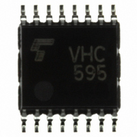
TC74VHC595FT(EL,M) Toshiba, TC74VHC595FT(EL,M) Datasheet

TC74VHC595FT(EL,M)
Specifications of TC74VHC595FT(EL,M)
Related parts for TC74VHC595FT(EL,M)
TC74VHC595FT(EL,M) Summary of contents
Page 1
... TOSHIBA CMOS Digital Integrated Circuit Silicon Monolithic TC74VHC595F,TC74VHC595FN,TC74VHC595FT,TC74VHC595FK 8-Bit Shift Register/Latch (3-state) The TC74VHC595 is an advanced high speed 8-BIT SHIFT REGISTER/LATCH fabricated with silicon gate C It achieves the high speed operation similar to equivalent Bipolar Schottky TTL while maintaining the CMOS low power dissipation. ...
Page 2
Pin Assignment GND 8 (top view) Truth Table Inputs SI SCK SCLR RCK ...
Page 3
Timing Chart SCK SI RCK SCLR QH’ System Diagram 10 SCLR SCK 11 SCK 12 RCK ...
Page 4
Absolute Maximum Ratings (Note) Characteristics Supply voltage range DC input voltage DC output voltage Input diode current Output diode current DC output current DC V /ground current CC Power dissipation Storage temperature Note: Exceeding any of the absolute maximum ratings, ...
Page 5
Electrical Characteristics DC Characteristics Characteristics Symbol High-level input V IH voltage Low-level input V IL voltage High-level output V OH voltage Low-level output V OL voltage 3-state output I OZ off-state current Input leakage I IN current Quiescent supply I ...
Page 6
Timing Requirements (input: t Characteristics Symbol Minimum pulse width (SCK, RCK) Minimum pulse width ( SCLR ) Minimum set-up time (SI-SCK) Minimum set-up time (SCK-RCK) Minimum set-up time ( SCLR -RCK) Minimum hold time (SI-SCK) Minimum hold time (SCK-RCK) Minimum ...
Page 7
AC Characteristics (input Characteristics Symbol Propagation delay t pLH time t pHL (SCK-QH’) Propagation delay time t pHL ( SCLR -QH’) Propagation delay t pLH time t pHL (RCK pZL Output enable time R t ...
Page 8
Noise Characteristics (input ns) Characteristics Quiet output maximum dynamic V OL Quiet output minimum dynamic V OL Minimum high level dynamic input voltage Maximum low level dynamic input voltage Input Equivalent Circuit INPUT Symbol Test ...
Page 9
Package Dimensions Weight: 0.18 g (typ.) TC74VHC595F/FN/FT/FK 9 2006-06-01 ...
Page 10
Package Dimensions Weight: 0.18 g (typ.) TC74VHC595F/FN/FT/FK 10 2006-06-01 ...
Page 11
Package Dimensions (Note) Note: This package is not available in Japan. Weight: 0.13 g (typ.) TC74VHC595F/FN/FT/FK 11 2006-06-01 ...
Page 12
Package Dimensions Weight: 0.06 g (typ.) TC74VHC595F/FN/FT/FK 12 2006-06-01 ...
Page 13
Package Dimensions Weight: 0.02 g (typ.) TC74VHC595F/FN/FT/FK 13 2006-06-01 ...
Page 14
... The information contained herein is presented only as a guide for the applications of our products. No responsibility is assumed by TOSHIBA for any infringements of patents or other rights of the third parties which may result from its use. No license is granted by implication or otherwise under any patents or other rights of TOSHIBA or the third parties. • ...


