74AHCT573PW,112 NXP Semiconductors, 74AHCT573PW,112 Datasheet
74AHCT573PW,112
Specifications of 74AHCT573PW,112
74AHCT573PW
935263074112


Related parts for 74AHCT573PW,112


74AHCT573PW,112 Summary of contents
Page 1
Octal D-type transparant latch; 3-state Rev. 6 — 25 November 2010 1. General description The 74AHC573; 74AHCT573 is a high-speed Si-gate CMOS device and is pin compatible with Low-power Schottky TTL (LSTTL specified in compliance with ...
Page 2
... NXP Semiconductors 3. Ordering information Table 1. Ordering information Type number Package Temperature range 74AHC573 40 C to +125 C 74AHC573D 40 C to +125 C 74AHC573PW 40 C to +125 C 74AHC573BQ 74AHCT573 40 C to +125 C 74AHCT573D 40 C to +125 C 74AHCT573PW 40 C to +125 C 74AHCT573BQ 4 ...
Page 3
... NXP Semiconductors Fig 2. Logic symbol LATCH LATCH Fig 4. Logic diagram 74AHC_AHCT573 Product data sheet mna807 Fig LATCH LATCH All information provided in this document is subject to legal disclaimers. Rev. 6 — 25 November 2010 74AHC573; 74AHCT573 Octal D-type transparant latch; 3-state EN1 mna808 IEC logic symbol ...
Page 4
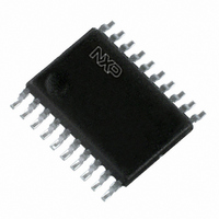
... NXP Semiconductors 5. Pinning information 5.1 Pinning 573 GND 001aad099 Fig 5. Pin configuration SO20 and TSSOP20 5.2 Pin description Table 2. Pin description Symbol Pin GND 19, 18, 17, 16, 15, 14, 13 74AHC_AHCT573 Product data sheet 74AHC573; 74AHCT573 (1) This is not a supply pin. The substrate is attached to this pad using conductive die attach material ...
Page 5
... NXP Semiconductors 6. Functional description [1] Table 3. Function table Operating mode Enable and read register (transparent mode) Latch and read register Latch register and disable outputs [ HIGH voltage level HIGH voltage level one set-up time prior to the HIGH-to-LOW LE transition LOW voltage level LOW voltage level one set-up time prior to the HIGH-to-LOW LE transition; ...
Page 6
... NXP Semiconductors 8. Recommended operating conditions Table 5. Operating conditions Symbol Parameter 74AHC573 V supply voltage CC V input voltage I V output voltage O T ambient temperature amb t/V input transition rise and fall rate 74AHCT573 V supply voltage CC V input voltage I V output voltage O T ambient temperature amb ...
Page 7
... NXP Semiconductors Table 6. Static characteristics At recommended operating conditions; voltages are referenced to GND (ground = 0 V). Symbol Parameter Conditions I OFF-state output current 5 input leakage current 5 supply current 5 input capacitance C output O capacitance 74AHCT573 V HIGH-level input voltage V LOW-level input voltage V HIGH-level output voltage = ...
Page 8
... NXP Semiconductors 10. Dynamic characteristics Table 7. Dynamic characteristics Voltages are referenced to GND (ground = 0 V); for test circuit see Symbol Parameter Conditions 74AHC573 t propagation Dn to Qn; see pd delay Qn; see enable time OE to Qn; see disable time OE to Qn; see ...
Page 9
... NXP Semiconductors Table 7. Dynamic characteristics Voltages are referenced to GND (ground = 0 V); for test circuit see Symbol Parameter Conditions t hold time Dn to LE; see power MHz dissipation V = GND capacitance 74AHCT573 4 5 propagation Dn to Qn; see pd delay Qn; see enable time OE to Qn; see disable time OE to Qn; see ...
Page 10
... NXP Semiconductors 11. Waveforms Measurement points are given in V and V are typical voltage output levels that occur with the output load Fig 7. Data input to output propagation delays LE input Qn output V and V are typical voltage output levels that occur with the output load Fig 8. ...
Page 11
... NXP Semiconductors OE input Qn output LOW-to-OFF OFF-to-LOW Qn output HIGH-to-OFF OFF-to-HIGH Measurement points are given in V and V are typical voltage output levels that occur with the output load Fig 9. Enable and disable times Dn input LE input Measurement points are given in V and V are typical voltage output levels that occur with the output load. ...
Page 12
... NXP Semiconductors negative Test data is given in Table Definitions test circuit termination resistance should be equal to output impedance load capacitance including jig and probe capacitance load resistance test selection switch. Fig 11. Test circuitry for switching times Table 9. Test data Type Input V I 74AHC573 ...
Page 13
... NXP Semiconductors 12. Package outline SO20: plastic small outline package; 20 leads; body width 7 pin 1 index 1 e DIMENSIONS (inch dimensions are derived from the original mm dimensions) A UNIT max. 0.3 2.45 mm 2.65 0.25 0.1 2.25 0.012 0.096 inches 0.1 0.01 0.004 0.089 Note 1. Plastic or metal protrusions of 0.15 mm (0.006 inch) maximum per side are not included. ...
Page 14
... NXP Semiconductors TSSOP20: plastic thin shrink small outline package; 20 leads; body width 4 pin 1 index 1 DIMENSIONS (mm are the original dimensions) A UNIT max. 0.15 0.95 mm 1.1 0.25 0.05 0.80 Notes 1. Plastic or metal protrusions of 0.15 mm maximum per side are not included. 2. Plastic interlead protrusions of 0.25 mm maximum per side are not included. ...
Page 15
... NXP Semiconductors DHVQFN20: plastic dual in-line compatible thermal enhanced very thin quad flat package; no leads; 20 terminals; body 2.5 x 4.5 x 0.85 mm terminal 1 index area terminal 1 index area DIMENSIONS (mm are the original dimensions) (1) A UNIT max. 0.05 0. 0.2 0.00 0.18 Note 1. Plastic or metal protrusions of 0.075 mm maximum per side are not included. ...
Page 16
... NXP Semiconductors 13. Abbreviations Table 10. Abbreviations Acronym Description CDM Charged Device Model CMOS Complementary Metal-Oxide Semiconductor ESD ElectroStatic Discharge HBM Human Body Model MM Machine Model TTL Transistor-Transistor Logic 14. Revision history Table 11. Revision history Document ID Release date 74AHC_AHCT573 v.6 20101125 • Modifications: Figure note [1] 74AHC_AHCT573 v ...
Page 17
... In no event shall NXP Semiconductors be liable for any indirect, incidental, punitive, special or consequential damages (including - without limitation - lost profits, lost savings, business interruption, costs related to the removal or ...
Page 18
... NXP Semiconductors Export control — This document as well as the item(s) described herein may be subject to export control regulations. Export might require a prior authorization from national authorities. 16. Contact information For more information, please visit: For sales office addresses, please send an email to: 74AHC_AHCT573 Product data sheet 74AHC573 ...
Page 19
... NXP Semiconductors 17. Contents 1 General description . . . . . . . . . . . . . . . . . . . . . . 1 2 Features and benefits . . . . . . . . . . . . . . . . . . . . 1 3 Ordering information . . . . . . . . . . . . . . . . . . . . . 2 4 Functional diagram . . . . . . . . . . . . . . . . . . . . . . 2 5 Pinning information . . . . . . . . . . . . . . . . . . . . . . 4 5.1 Pinning . . . . . . . . . . . . . . . . . . . . . . . . . . . . . . . 4 5.2 Pin description . . . . . . . . . . . . . . . . . . . . . . . . . 4 6 Functional description . . . . . . . . . . . . . . . . . . . 5 7 Limiting values Recommended operating conditions Static characteristics Dynamic characteristics . . . . . . . . . . . . . . . . . . 8 11 Waveforms . . . . . . . . . . . . . . . . . . . . . . . . . . . . 10 12 Package outline . . . . . . . . . . . . . . . . . . . . . . . . 13 13 Abbreviations ...