NLX1G99BMX1TCG ON Semiconductor, NLX1G99BMX1TCG Datasheet - Page 10
NLX1G99BMX1TCG
Manufacturer Part Number
NLX1G99BMX1TCG
Description
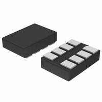
IC MINIGATE MULTIFUNC 8ULLGA
Manufacturer
ON Semiconductor
Datasheet
1.NLX1G99AMX1TCG.pdf
(15 pages)
Specifications of NLX1G99BMX1TCG
Logic Type
Configurable Multiple Function
Number Of Circuits
1
Number Of Inputs
4
Schmitt Trigger Input
Yes
Output Type
Tri-State
Current - Output High, Low
32mA, 32mA
Voltage - Supply
1.65 V ~ 5.5 V
Operating Temperature
-55°C ~ 125°C
Mounting Type
Surface Mount
Package / Case
8-ULLGA
Lead Free Status / RoHS Status
Lead free / RoHS Compliant


7. Waveform 1 is for an output with internal conditions such that the output is low, except when disabled by the output control.
8. All input pulses are supplied by generators having the following characteristics: PRR v 10 MHz, Z
9. The outputs are measured one at a time, with one transition per measurement.
10. All parameters are waveforms are not applicable to all devices.
From Output
Under Test
Figure 20. Voltage Waveforms Propagation Delay
Waveform 2 is for an output with internal conditions such that the output is high, except when disabled by the output control
*C
Figure 18. Voltage Waveforms Pulse Duration
C
L
Input
L
Times Inverting and Noninverting Outputs
includes probes and jig capacitance.
*
Output
Output
Input
R
L
t
t
Figure 17. Load Circuit
PLH
PHL
1.8 V $ 0.15 V
2.5 V $ 0.2 V
3.3 V $ 0.3 V
5.5 V $ 0.5 V
V
V
M
V
M
CC
R
t
W
L
V
V
M
M
TEST CIRCUIT AND VOLTAGE WAVEFORMS
V
M
V
V
V
3 V
V
S1
CC
CC
CC
t
t
I
V
PHL
PLH
V
V
M
Inputs
M
M
v 2.5 ns
v 2.5 ns
V
0 V
V
V
V
V
v 2 ns
v 2 ns
I
OH
OL
OH
OL
t
V
0 V
V
GND
r
/t
I
LOAD
f
Open
http://onsemi.com
V
V
V
1.5 V
V
CC
CC
CC
M
/2
/2
/2
10
S1 at V
2 x V
2 x V
2 x V
Waveform 1
Waveform 2
V
S1 at GND
Timing Input
LOAD
6 V
Data Input
(Note 7)
(Note 7)
Figure 19. Voltage Waveforms Setup and Hold
Disable Times Low− and High−Level Enabling
Control
CC
CC
CC
Output
Output
Output
Figure 21. Voltage Waveforms Enable and
LOAD
t
15 pF
15 pF
15 pF
15 pF
PZH
C
t
t
t
PLH
PHZ
PLZ
L
Test
/t
/t
/t
PHL
PZL
PZH
1 MW
1 MW
1 MW
1 MW
R
V
L
M
t
su
V
V
V
M
Times
M
M
O
= 50 W.
V
0.15 V
0.15 V
t
M
h
0.3 V
0.3 V
V
V
D
M
V
V
OL
OH
V
t
PHZ
M
+ V
− V
V
0 V
V
Open
GND
D
V
V
V
D
[0 V
I
LOAD
S1
V
0 V
V
0 V
LOAD
OL
OH
I
I
/2
Related parts for NLX1G99BMX1TCG
Image
Part Number
Description
Manufacturer
Datasheet
Request
R

Part Number:
Description:
ON Semiconductor [VOLTAGE REGULATOR]
Manufacturer:
ON Semiconductor
Datasheet:
Part Number:
Description:
357-036-542-201 CARDEDGE 36POS DL .156 BLK LOPRO
Manufacturer:
ON Semiconductor
Datasheet:
Part Number:
Description:
357-036-542-201 CARDEDGE 36POS DL .156 BLK LOPRO
Manufacturer:
ON Semiconductor
Datasheet:
Part Number:
Description:
357-036-542-201 CARDEDGE 36POS DL .156 BLK LOPRO
Manufacturer:
ON Semiconductor
Datasheet:
Part Number:
Description:
357-036-542-201 CARDEDGE 36POS DL .156 BLK LOPRO
Manufacturer:
ON Semiconductor
Datasheet:
Part Number:
Description:
357-036-542-201 CARDEDGE 36POS DL .156 BLK LOPRO
Manufacturer:
ON Semiconductor
Datasheet:
Part Number:
Description:
357-036-542-201 CARDEDGE 36POS DL .156 BLK LOPRO
Manufacturer:
ON Semiconductor
Datasheet:
Part Number:
Description:
357-036-542-201 CARDEDGE 36POS DL .156 BLK LOPRO
Manufacturer:
ON Semiconductor
Datasheet:
Part Number:
Description:
357-036-542-201 CARDEDGE 36POS DL .156 BLK LOPRO
Manufacturer:
ON Semiconductor
Datasheet:
Part Number:
Description:
357-036-542-201 CARDEDGE 36POS DL .156 BLK LOPRO
Manufacturer:
ON Semiconductor
Datasheet:
Part Number:
Description:
357-036-542-201 CARDEDGE 36POS DL .156 BLK LOPRO
Manufacturer:
ON Semiconductor
Datasheet:
Part Number:
Description:
Manufacturer:
ON Semiconductor
Datasheet:
Part Number:
Description:
Manufacturer:
ON Semiconductor
Datasheet:
Part Number:
Description:
Manufacturer:
ON Semiconductor
Datasheet: