MC74ACT00DR2G ON Semiconductor, MC74ACT00DR2G Datasheet - Page 2
MC74ACT00DR2G
Manufacturer Part Number
MC74ACT00DR2G
Description
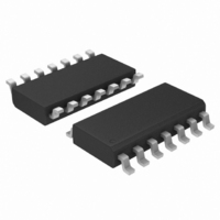
IC GATE NAND QUAD 2INPUT 14SOIC
Manufacturer
ON Semiconductor
Series
74ACTr
Datasheet
1.MC74AC00DG.pdf
(10 pages)
Specifications of MC74ACT00DR2G
Logic Type
NAND Gate
Number Of Inputs
2
Number Of Circuits
4
Current - Output High, Low
24mA, 24mA
Voltage - Supply
4.5 V ~ 5.5 V
Operating Temperature
-40°C ~ 85°C
Mounting Type
Surface Mount
Package / Case
14-SOIC (3.9mm Width), 14-SOL
Logic Family
ACT
Logical Function
NAND
Number Of Elements
4
High Level Output Current
-24mA
Low Level Output Current
24mA
Propagation Delay Time
9.5ns
Operating Supply Voltage (typ)
5V
Operating Temp Range
-55C to 125C
Package Type
SOIC
Number Of Outputs
1
Technology
CMOS
Mounting
Surface Mount
Pin Count
14
Operating Temperature Classification
Military
Quiescent Current
4uA
Operating Supply Voltage (max)
5.5V
Operating Supply Voltage (min)
4.5V
Lead Free Status / RoHS Status
Lead free / RoHS Compliant
Other names
MC74ACT00DR2GOS
Available stocks
Company
Part Number
Manufacturer
Quantity
Price
Company:

Part Number:
MC74ACT00DR2G
Manufacturer:
ON Semiconductor
Quantity:
500


Stresses exceeding Maximum Ratings may damage the device. Maximum Ratings are stress ratings only. Functional operation above the
Recommended Operating Conditions is not implied. Extended exposure to stresses above the Recommended Operating Conditions may affect
device reliability.
1. I
2. Tested to EIA/JESD22−A114−A.
3. Tested to EIA/JESD22−A115−A.
4. Tested to JESD22−C101−A.
5. Tested to EIA/JESD78.
RECOMMENDED OPERATING CONDITIONS
MAXIMUM RATINGS
6. V
7. V
V
V
V
I
I
I
I
I
T
T
T
q
P
MSL
F
V
I
V
V
t
t
T
T
I
I
Symbol
IK
OK
O
CC
GND
Latch−Up
r
r
OH
OL
JA
, t
, t
A
STG
L
J
R
J
CC
I
O
D
ESD
CC
in
Symbol
O
, V
f
f
in
in
absolute maximum rating must be observed.
out
from 30% to 70% V
from 0.8 V to 2.0 V.
DC Supply Voltage
DC Input Voltage
DC Output Voltage
DC Input Diode Current
DC Output Diode Current
DC Output Sink/Source Current
DC Supply Current per Output Pin
DC Ground Current per Output Pin
Storage Temperature Range
Lead temperature, 1 mm from Case for 10 Seconds
Junction temperature under Bias
Thermal resistance
Power Dissipation in Still Air at 85°C
Moisture Sensitivity
Flammability Rating
ESD Withstand Voltage
Latch−Up Performance
DC Input Voltage, Output Voltage (Ref. to GND)
Junction Temperature
Operating Ambient Temperature Range
Output Current − High
Output Current − Low
Supply Voltage
Input Rise and Fall Time (Note 6)
MC74AC00
Input Rise and Fall Time (Note 7)
MC74ACT00
CC
.
Above V
Parameter
CC
Parameter
and Below GND at 85°C (Note 5)
Charged Device Model (Note 4)
Human Body Model (Note 2)
Oxygen Index: 30% − 35%
http://onsemi.com
Machine Model (Note 3)
2
MC74ACT00
V
V
V
V
V
MC74AC00
CC
CC
CC
CC
CC
(Note 1)
@ 3.0 V
@ 4.5 V
@ 5.5 V
@ 4.5 V
@ 5.5 V
TSSOP
TSSOP
SOIC
SOIC
PDIP
PDIP
Min
−55
2.0
4.5
0
−
−
−
−
−
−
−
−
*0.5 v V
*0.5 v V
UL 94 V−0 @ 0.125 in
Typ
150
5.0
5.0
8.0
40
25
10
25
−
−
−
−
*0.5 to )7.0
*65 to )150
Level 1
> 2000
> 1000
Value
)150
$100
> 200
$20
$50
$50
$50
$50
O
I
260
125
170
125
170
78
78
v V
v V
Max
V
150
125
−24
6.0
5.5
24
CC
CC
CC
−
−
−
−
−
)0.5
)0.5
Unit
ns/V
ns/V
mA
mA
°C
°C
V
V
°C/W
Unit
mW
mA
mA
mA
mA
mA
mA
°C
°C
°C
V
V
V
V
Related parts for MC74ACT00DR2G
Image
Part Number
Description
Manufacturer
Datasheet
Request
R

Part Number:
Description:
ON Semiconductor [VOLTAGE REGULATOR]
Manufacturer:
ON Semiconductor
Datasheet:
Part Number:
Description:
357-036-542-201 CARDEDGE 36POS DL .156 BLK LOPRO
Manufacturer:
ON Semiconductor
Datasheet:
Part Number:
Description:
357-036-542-201 CARDEDGE 36POS DL .156 BLK LOPRO
Manufacturer:
ON Semiconductor
Datasheet:
Part Number:
Description:
357-036-542-201 CARDEDGE 36POS DL .156 BLK LOPRO
Manufacturer:
ON Semiconductor
Datasheet:
Part Number:
Description:
357-036-542-201 CARDEDGE 36POS DL .156 BLK LOPRO
Manufacturer:
ON Semiconductor
Datasheet:
Part Number:
Description:
357-036-542-201 CARDEDGE 36POS DL .156 BLK LOPRO
Manufacturer:
ON Semiconductor
Datasheet:
Part Number:
Description:
357-036-542-201 CARDEDGE 36POS DL .156 BLK LOPRO
Manufacturer:
ON Semiconductor
Datasheet:
Part Number:
Description:
357-036-542-201 CARDEDGE 36POS DL .156 BLK LOPRO
Manufacturer:
ON Semiconductor
Datasheet:
Part Number:
Description:
357-036-542-201 CARDEDGE 36POS DL .156 BLK LOPRO
Manufacturer:
ON Semiconductor
Datasheet:
Part Number:
Description:
357-036-542-201 CARDEDGE 36POS DL .156 BLK LOPRO
Manufacturer:
ON Semiconductor
Datasheet:
Part Number:
Description:
357-036-542-201 CARDEDGE 36POS DL .156 BLK LOPRO
Manufacturer:
ON Semiconductor
Datasheet:
Part Number:
Description:
Manufacturer:
ON Semiconductor
Datasheet:
Part Number:
Description:
Manufacturer:
ON Semiconductor
Datasheet:
Part Number:
Description:
Manufacturer:
ON Semiconductor
Datasheet: