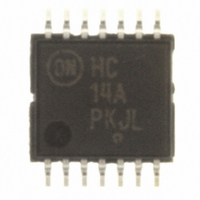
MC74HC14ADTR2G ON Semiconductor, MC74HC14ADTR2G Datasheet

MC74HC14ADTR2G
Specifications of MC74HC14ADTR2G
Available stocks
Related parts for MC74HC14ADTR2G
MC74HC14ADTR2G Summary of contents
Page 1
MC74HC14A Hex Schmitt−Trigger Inverter High−Performance Silicon−Gate CMOS The MC74HC14A is identical in pinout to the LS14, LS04 and the HC04. The device inputs are compatible with Standard CMOS outputs; with pullup resistors, they are compatible with LSTTL outputs. The HC14A ...
Page 2
... Device MC74HC14AN MC74HC14ANG MC74HC14AD MC74HC14ADG MC74HC14ADR2 MC74HC14ADR2G MC74HC14ADT MC74HC14ADTG MC74HC14ADTR2 MC74HC14ADTR2G MC74HC14AF MC74HC14AFG MC74HC14AFEL MC74HC14AFELG †For information on tape and reel specifications, including part orientation and tape sizes, please refer to our Tape and Reel Packaging Specifications Brochure, BRD8011/D. *This package is inherently Pb−Free ...
Page 3
... SOIC Package: – 7 mW/_C from 65_ to 125_C TSSOP Package: − 6.1 mW/_C from 65_ to 125_C For high frequency or heavy load considerations, see Chapter 2 of the ON Semiconductor High−Speed CMOS Data Book (DL129/D). RECOMMENDED OPERATING CONDITIONS Symbol Parameter Î ...
Page 4
DC CHARACTERISTICS (Voltages Referenced to GND) Symbol Parameter V max Maximum Positive−Going Input T+ Threshold Voltage (Figure 3) V min Minimum Positive−Going Input T+ Threshold Voltage (Figure 3) V max Maximum Negative−Going Input T− Threshold Voltage (Figure 3) V min ...
Page 5
... NOTE: For propagation delays with loads other than 50 pF, and information on typical parametric values, see Chapter 2 of the ON Semiconductor High−Speed CMOS Data Book (DL129/D). C Power Dissipation Capacitance (Per Inverter Used to determine the no−load dynamic power consumption Semiconductor High−Speed CMOS Data Book (DL129/D). INPUT A OUTPUT 6ns) r ...
Page 6
Figure 3. Typical Input Threshold, V (a) A Schmitt−Trigger Squares Up Inputs With Slow Rise and Fall Times out Figure 4. Typical Schmitt−Trigger Applications ( T− ...
Page 7
−T− SEATING PLANE 0.13 (0.005) PACKAGE DIMENSIONS PDIP−14 CASE 646−06 ISSUE http://onsemi.com 7 NOTES: 1. DIMENSIONING AND TOLERANCING PER ANSI ...
Page 8
... G −T− SEATING 14 PL PLANE 0.25 (0.010 14X 0.58 *For additional information on our Pb−Free strategy and soldering details, please download the ON Semiconductor Soldering and Mounting Techniques Reference Manual, SOLDERRM/D. PACKAGE DIMENSIONS SOIC−14 CASE 751A−03 ISSUE 0.25 (0.010 ...
Page 9
... S A −V− C 0.10 (0.004) −T− SEATING G D PLANE 14X 0.36 *For additional information on our Pb−Free strategy and soldering details, please download the ON Semiconductor Soldering and Mounting Techniques Reference Manual, SOLDERRM/D. PACKAGE DIMENSIONS TSSOP−14 CASE 948G−01 ISSUE 0.25 (0.010) ...
Page 10
... Opportunity/Affirmative Action Employer. This literature is subject to all applicable copyright laws and is not for resale in any manner. PUBLICATION ORDERING INFORMATION LITERATURE FULFILLMENT: Literature Distribution Center for ON Semiconductor P.O. Box 5163, Denver, Colorado 80217 USA Phone: 303−675−2175 or 800−344−3860 Toll Free USA/Canada Fax: 303− ...


