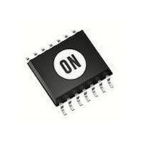
MC74HCT04ADTR2G ON Semiconductor, MC74HCT04ADTR2G Datasheet - Page 4

MC74HCT04ADTR2G
Manufacturer Part Number
MC74HCT04ADTR2G
Description
IC INVERTER HEX LSTTL IN 14TSSOP
Manufacturer
ON Semiconductor
Series
74HCTr
Datasheet
1.MC74HCT04ADTR2G.pdf
(8 pages)
Specifications of MC74HCT04ADTR2G
Logic Type
Inverter
Number Of Inputs
1
Number Of Circuits
6
Current - Output High, Low
4mA, 4mA
Voltage - Supply
4.5 V ~ 5.5 V
Operating Temperature
-55°C ~ 125°C
Mounting Type
Surface Mount
Package / Case
14-TSSOP
Logic Family
74HCT
High Level Output Current
- 4 mA
Low Level Output Current
4 mA
Supply Voltage (max)
5.5 V
Supply Voltage (min)
4.5 V
Maximum Operating Temperature
+ 125 C
Mounting Style
SMD/SMT
Operating Supply Voltage
2 V to 6 V
Output Current
4mA
No. Of Inputs
1
Supply Voltage Range
4.5V To 5.5V
Logic Case Style
TSSOP
No. Of Pins
14
Operating Temperature Range
-55°C To +125°C
Termination Type
SMD
Rohs Compliant
Yes
Filter Terminals
SMD
Family Type
HC
Lead Free Status / RoHS Status
Lead free / RoHS Compliant
Available stocks
Company
Part Number
Manufacturer
Quantity
Price
Company:
Part Number:
MC74HCT04ADTR2G
Manufacturer:
ON Semiconductor
Quantity:
9 700
3. For propagation delays with loads other than 50 pF, and information on typical parametric values, see Chapter 2 of the ON Semiconductor
* Used to determine the no−load dynamic power consumption: P
AC CHARACTERISTICS
Symbol
ON Semiconductor High−Speed CMOS Data Book (DL129/D).
t
t
t
C
t
OUTPUT Y
PLH
High−Speed CMOS Data Book (DL129/D).
TLH
PHL
THL
C
PD
in
INPUT A
,
,
Maximum Propagation Delay, Input A to Output Y
(Figures 1 and 2)
Maximum Output Transition Time, Any Output
(Figures 1 and 2)
Maximum Input Capacitance
Power Dissipation Capacitance (Per Inverter)*
2.7V
1.3V
0.3V
t
PLH
t
TLH
10%
Figure 1. Switching Waveforms
1.3V
90%
(V
CC
t
f
= 5.0V ±10%, C
t
r
Parameter
A
Figure 3. Expanded Logic Diagram
L
= 50pF, Input t
(1/6 of the Device Shown)
http://onsemi.com
t
PHL
D
r
= C
= t
4
t
THL
f
3.0V
GND
PD
= 6ns)
V
CC
2
f + I
CC
V
CC
−55 to 25°C
. For load considerations, see Chapter 2 of the
15
17
15
10
Typical @ 25°C, V
Y
*Includes all probe and jig capacitance
Guaranteed Limit
Figure 2. Test Circuit
DEVICE
UNDER
TEST
≤85°C
22
19
21
19
10
CC
= 5.0 V
OUTPUT
≤125°C
22
26
22
10
POINT
TEST
C
Unit
pF
pF
ns
ns
L
*


