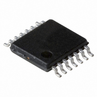
74ABT04DB,112 NXP Semiconductors, 74ABT04DB,112 Datasheet - Page 4

74ABT04DB,112
Manufacturer Part Number
74ABT04DB,112
Description
IC HEX INVERTER 14-SSOP
Manufacturer
NXP Semiconductors
Series
74ABTr
Datasheet
1.74ABT04D118.pdf
(10 pages)
Specifications of 74ABT04DB,112
Number Of Circuits
6
Logic Type
Inverter
Package / Case
14-SSOP
Number Of Inputs
1
Current - Output High, Low
15mA, 20mA
Voltage - Supply
4.5 V ~ 5.5 V
Operating Temperature
-40°C ~ 85°C
Mounting Type
Surface Mount
Logic Family
74ABT
High Level Output Current
- 15 mA
Low Level Output Current
20 mA
Propagation Delay Time
2.2 ns
Supply Voltage (max)
5.5 V
Supply Voltage (min)
4.5 V
Maximum Operating Temperature
+ 85 C
Minimum Operating Temperature
- 40 C
Mounting Style
SMD/SMT
Operating Supply Voltage
5 V
Lead Free Status / RoHS Status
Lead free / RoHS Compliant
Lead Free Status / RoHS Status
Lead free / RoHS Compliant, Lead free / RoHS Compliant
Other names
568-2467-5
935207000112
935207000112
1. Skew is defined as the absolute value of the difference between the actual propagation delay for any two separate outputs of the same
Philips Semiconductors
AC CHARACTERISTICS
GND = 0V; t
NOTE:
AC WAVEFORMS
V
TEST CIRCUIT AND WAVEFORMS
1995 Sep 18
M
SYMBOL
Hex inverter
device. The specification applies to any outputs switching in the the same direction, either HIGH-to-LOW (t
parameter guaranteed by design.
t
= 1.5V, V
t
OSLH
DEFINITIONS
R
C
R
t
t
OSHL
PLH
PHL
Waveform 1. Propagation delay for inverting outputs
GENERATOR
T
L
L
= Load resistor; see AC CHARACTERISTICS for value.
= Load capacitance includes jig and probe capacitance;
= Termination resistance should be equal to Z
An
PULSE
Yn
1
see AC CHARACTERISTICS for value.
pulse generators.
R
IN
= t
Propagation delay
An to Yn
Output to Output skew
An or Bn to Yn
= GND to 3.0V
F
= 2.5ns; C
V
IN
Test Circuit for Outputs
R
PARAMETER
T
V
M
t
L
PHL
= 50pF, R
V
M
D.U.T.
V
CC
V
M
L
= 500
V
OUT
t
PLH
C
V
L
M
OUT
WAVEFORM
SA00341
R
L
of
1
2
4
FAMILY
74ABT
MIN
1.0
1.0
NEGATIVE
PULSE
POSITIVE
PULSE
T
INPUT
OUTPUT
V
OUTPUT N
same part
amb
90%
10%
CC
Amplitude
TYP
= +5.0V
2.2
1.6
0.4
= +25 C
3.0V
Waveform 2. Common edge skew
V
V
M
Input Pulse Definition
10%
90%
M
INPUT PULSE REQUIREMENTS
MAX
t
t
THL
TLH
3.4
2.5
0.5
LIMITS
t
PLH
V
Rep. Rate
(t
(t
F
R
M
MIN
1MHz
)
t
)
PLH
= 1.5V
t
t
W
W
T
amb
MAX
t
V
OSLH
MIN
1.0
1.0
CC
OSHL
= –40 C to +85 C
= +5.0V 0.5V
10%
90%
500ns
) or LOW-to-HIGH (t
t
W
V
V
M
M
t
PHL
MIN
MAX
t
Product Specification
PHL
4.1
3.0
0.5
2.5ns
74ABT04
t
90%
10%
R
MAX
t
OSHL
t
t
TLH
THL
SA00381
(t
(t
2.5ns
SH00067
0V
0V
AMP (V)
AMP (V)
R
F
t
F
)
UNIT
)
OSLH
ns
ns
);


