MC14069UBCPG ON Semiconductor, MC14069UBCPG Datasheet
MC14069UBCPG
Specifications of MC14069UBCPG
Available stocks


Related parts for MC14069UBCPG

MC14069UBCPG Summary of contents
Page 1
MC14069UB Hex Inverter The MC14069UB hex inverter is constructed with MOS P−channel and N−channel enhancement mode devices in a single monolithic structure. These inverters find primary use where low power dissipation and/or high noise immunity is desired. Each of the ...
Page 2
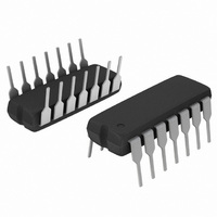
... PULSE GENERATOR INPUT 7 V Figure 4. Switching Time Test Circuit and Waveforms ORDERING INFORMATION Device MC14069UBCP MC14069UBCPG MC14069UBD MC14069UBDG MC14069UBDR2 MC14069UBDR2G MC14069UBDTR2 MC14069UBDTR2G MC14069UBFEL MC14069UBFELG †For information on tape and reel specifications, including part orientation and tape sizes, please refer to our Tape and Reel Packaging Specifications Brochure, BRD8011/D. *This package is inherently Pb− ...
Page 3
ELECTRICAL CHARACTERISTICS Î Î Î Î Î ...
Page 4
−T− SEATING PLANE 0.13 (0.005) PACKAGE DIMENSIONS PDIP−14 CASE 646−06 ISSUE NOTES: 1. DIMENSIONING AND TOLERANCING PER ANSI Y14.5M, ...