MC74HC03ADG ON Semiconductor, MC74HC03ADG Datasheet - Page 2
MC74HC03ADG
Manufacturer Part Number
MC74HC03ADG
Description
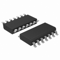
IC GATE NAND QUAD 2INP 14-SOIC
Manufacturer
ON Semiconductor
Series
74HCr
Specifications of MC74HC03ADG
Logic Type
NAND Gate with Open Drain
Number Of Inputs
2
Number Of Circuits
4
Current - Output High, Low
5.2mA, 5.2mA
Voltage - Supply
2 V ~ 6 V
Operating Temperature
-55°C ~ 125°C
Mounting Type
Surface Mount
Package / Case
14-SOIC (3.9mm Width), 14-SOL
Output Current
5.2mA
No. Of Inputs
2
Supply Voltage Range
2V To 6V
Logic Case Style
SOIC
No. Of Pins
14
Operating Temperature Range
-55°C To +125°C
Filter Terminals
SMD
Rohs Compliant
Yes
Family Type
HC
Lead Free Status / RoHS Status
Lead free / RoHS Compliant
Other names
MC74HC03ADG
MC74HC03ADGOS
MC74HC03ADGOS


Î Î Î Î Î Î Î Î Î Î Î Î Î Î Î Î Î Î Î Î Î Î Î
Î Î Î Î Î Î Î Î Î Î Î Î Î Î Î Î Î Î Î Î Î Î Î
Î Î Î Î
Î Î Î Î
Î Î Î Î
Î Î Î Î
Î Î Î Î
Î Î Î Î
Î Î Î Î
Î Î Î Î
Î Î Î Î
Î Î Î Î
Î Î Î Î
Î Î Î Î
Î Î Î Î
Î Î Î Î
Î Î Î Î
Î Î Î Î
Î Î Î Î
Î Î Î Î
Î Î Î Î
Î Î Î Î
Î Î Î Î
Î Î Î Î
Î Î Î Î
Î Î Î Î
Î Î Î Î
Î Î Î Î
Î Î Î Î
Î Î Î Î
Î Î Î Î
Î Î Î Î
Î Î Î Î
Stresses exceeding Maximum Ratings may damage the device. Maximum Ratings are stress
ratings only. Functional operation above the Recommended Operating Conditions is not implied.
Extended exposure to stresses above the Recommended Operating Conditions may affect device
reliability.
†Derating — Plastic DIP: – 10 mW/_C from 65_ to 125_C
For high frequency or heavy load considerations, see Chapter 2 of the ON Semiconductor High−Speed CMOS Data Book (DL129/D).
DESIGN GUIDE
*Equivalent to a two−input NAND gate
MAXIMUM RATINGS
RECOMMENDED OPERATING CONDITIONS
Symbol
Symbol
V
Internal Gate Count*
Internal Gate Propagation Delay
Internal Gate Power Dissipation
Speed Power Product
in
V
V
V
T
t
I
I
V
P
T
, V
T
r
I
out
CC
CC
out
stg
CC
, t
in
in
D
A
L
f
out
Î Î Î Î Î Î Î Î Î Î Î Î Î Î
Î Î Î Î Î Î Î Î Î Î Î Î Î Î
Î Î Î Î Î Î Î Î Î Î Î Î Î Î
Î Î Î Î Î Î Î Î Î Î Î Î Î Î
Î Î Î Î Î Î Î Î Î Î Î Î Î Î
Î Î Î Î Î Î Î Î Î Î Î Î Î Î
Î Î Î Î Î Î Î Î Î Î Î Î Î Î
Î Î Î Î Î Î Î Î Î Î Î Î Î Î
Î Î Î Î Î Î Î Î Î Î Î Î Î Î
Î Î Î Î Î Î Î Î Î Î Î Î Î Î
Î Î Î Î Î Î Î Î Î Î Î Î Î Î
Î Î Î Î Î Î Î Î Î Î Î Î Î Î
Î Î Î Î Î Î Î Î Î Î Î Î Î Î
Î Î Î Î Î Î Î Î Î Î Î Î Î Î
Î Î Î Î Î Î Î Î Î Î Î Î Î Î
Î Î Î Î Î Î Î Î Î Î Î Î Î Î
Î Î Î Î Î Î Î Î Î Î Î Î Î Î
Î Î Î Î Î Î Î Î Î Î Î Î Î Î
Î Î Î Î Î Î Î Î Î Î Î Î Î Î
Î Î Î Î Î Î Î Î Î Î Î Î Î Î
Î Î Î Î Î Î Î Î Î Î Î Î Î Î
Î Î Î Î Î Î Î Î Î Î Î Î Î Î
Î Î Î Î Î Î Î Î Î Î Î Î Î Î
Î Î Î Î Î Î Î Î Î Î Î Î Î Î
Î Î Î Î Î Î Î Î Î Î Î Î Î Î
Î Î Î Î Î Î Î Î Î Î Î Î Î Î
Î Î Î Î Î Î Î Î Î Î Î Î Î Î
Î Î Î Î Î Î Î Î Î Î Î Î Î Î
Î Î Î Î Î Î Î Î Î Î Î Î Î Î
Î Î Î Î Î Î Î Î Î Î Î Î Î Î
Î Î Î Î Î Î Î Î Î Î Î Î Î Î
DC Supply Voltage (Referenced to GND)
DC Input Voltage (Referenced to GND)
DC Output Voltage (Referenced to GND)
DC Input Current, per Pin
DC Output Current, per Pin
DC Supply Current, V
Power Dissipation in Still Air
Storage Temperature
Lead Temperature, 1 mm from Case for 10 Seconds
DC Supply Voltage (Referenced to GND)
DC Input Voltage, Output Voltage (Referenced to GND)
Operating Temperature, All Package Types
Input Rise and Fall Time
(Figure 1)
SOIC Package: – 7 mW/_C from 65_ to 125_C
TSSOP Package: − 6.1 mW/_C from 65_ to 125_C
Plastic DIP, SOIC or TSSOP Package
Criteria
Parameter
Parameter
CC
and GND Pins
TSSOP Package†
SOIC Package†
Plastic DIP†
V
V
V
CC
CC
CC
= 2.0 V
= 4.5 V
= 6.0 V
http://onsemi.com
Î Î Î Î Î Î
Î Î Î Î Î Î
Î Î Î Î Î Î
Î Î Î Î Î Î
Î Î Î Î Î Î
Î Î Î Î Î Î
Î Î Î Î Î Î
Î Î Î Î Î Î
Î Î Î Î Î Î
Î Î Î Î Î Î
Î Î Î Î Î Î
Î Î Î Î Î Î
Î Î Î Î Î Î
Î Î Î Î Î Î
Î Î Î Î Î Î
Î Î Î Î Î Î
Î Î Î Î Î Î
Î Î Î Î Î Î
Î Î Î Î Î Î
Î Î Î Î Î Î
Î Î Î Î Î Î
Î Î Î
Î Î Î
Î Î Î
Î Î Î
Î Î Î
Î Î Î
Î Î Î
Î Î Î
Î Î Î
Î Î Î
– 0.5 to V
– 0.5 to V
2
– 55
Min
2.0
– 0.5 to + 7.0
– 65 to + 150
0
0
0
0
0.0075
Value
Value
Î Î Î Î
Î Î Î Î
Î Î Î Î
Î Î Î Î
Î Î Î Î
Î Î Î Î
Î Î Î Î
Î Î Î Î
Î Î Î Î
Î Î Î Î
± 20
± 25
± 50
750
500
450
260
7.0
1.5
5.0
CC
CC
+ 125
1000
Max
V
500
400
6.0
+ 0.5
+ 0.5
CC
Î Î
Î Î
Î Î
Î Î
Î Î
Î Î Î Î
Î Î Î Î
Î Î Î Î
Î Î Î Î
Î Î
Î Î
Î Î
Î Î
Î Î
Î Î
Î Î Î Î
Î Î
Î Î
Î Î
Î Î
Î Î
Î Î
Î Î
Î Î
Î Î Î Î
Unit
Unit
Unit
mW
mA
mA
mA
mW
_C
_C
_C
ea
ns
ns
pJ
V
V
V
V
V
circuitry to guard against damage
due to high static voltages or electric
fields. However, precautions must
be taken to avoid applications of any
voltage higher than maximum rated
voltages to this high−impedance cir-
cuit. For proper operation, V
V
range GND v (V
tied to an appropriate logic voltage
level (e.g., either GND or V
Unused outputs must be left open.
out
This device contains protection
Unused inputs must always be
should be constrained to the
in
or V
out
) v V
in
CC
CC
and
.
).
Related parts for MC74HC03ADG
Image
Part Number
Description
Manufacturer
Datasheet
Request
R

Part Number:
Description:
CONTACTOR, 110VAC, 74A, DIN RAIL
Manufacturer:
IMO PRECISION CONTROLS
Datasheet:
Part Number:
Description:
CONTACTOR, 230VAC, 74A, DIN RAIL
Manufacturer:
IMO PRECISION CONTROLS
Datasheet:
Part Number:
Description:
CONTACTOR, 24VAC, 74A, DIN RAIL
Manufacturer:
IMO PRECISION CONTROLS
Datasheet:

Part Number:
Description:
ON Semiconductor [VOLTAGE REGULATOR]
Manufacturer:
ON Semiconductor
Datasheet:
Part Number:
Description:
357-036-542-201 CARDEDGE 36POS DL .156 BLK LOPRO
Manufacturer:
ON Semiconductor
Datasheet:
Part Number:
Description:
357-036-542-201 CARDEDGE 36POS DL .156 BLK LOPRO
Manufacturer:
ON Semiconductor
Datasheet:
Part Number:
Description:
357-036-542-201 CARDEDGE 36POS DL .156 BLK LOPRO
Manufacturer:
ON Semiconductor
Datasheet:
Part Number:
Description:
357-036-542-201 CARDEDGE 36POS DL .156 BLK LOPRO
Manufacturer:
ON Semiconductor
Datasheet:
Part Number:
Description:
357-036-542-201 CARDEDGE 36POS DL .156 BLK LOPRO
Manufacturer:
ON Semiconductor
Datasheet:
Part Number:
Description:
357-036-542-201 CARDEDGE 36POS DL .156 BLK LOPRO
Manufacturer:
ON Semiconductor
Datasheet:
Part Number:
Description:
357-036-542-201 CARDEDGE 36POS DL .156 BLK LOPRO
Manufacturer:
ON Semiconductor
Datasheet:
Part Number:
Description:
357-036-542-201 CARDEDGE 36POS DL .156 BLK LOPRO
Manufacturer:
ON Semiconductor
Datasheet:
Part Number:
Description:
357-036-542-201 CARDEDGE 36POS DL .156 BLK LOPRO
Manufacturer:
ON Semiconductor
Datasheet:
Part Number:
Description:
357-036-542-201 CARDEDGE 36POS DL .156 BLK LOPRO
Manufacturer:
ON Semiconductor
Datasheet: