74AHC00PW,118 NXP Semiconductors, 74AHC00PW,118 Datasheet - Page 2
74AHC00PW,118
Manufacturer Part Number
74AHC00PW,118
Description
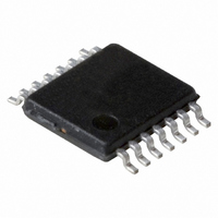
IC QUAD 2-IN NAND GATE 14TSSOP
Manufacturer
NXP Semiconductors
Series
74AHCr
Datasheet
1.74AHC00PW118.pdf
(14 pages)
Specifications of 74AHC00PW,118
Number Of Circuits
4
Package / Case
14-TSSOP
Logic Type
NAND Gate
Number Of Inputs
2
Current - Output High, Low
8mA, 8mA
Voltage - Supply
2 V ~ 5.5 V
Operating Temperature
-40°C ~ 125°C
Mounting Type
Surface Mount
Product
NAND
Logic Family
AHC
High Level Output Current
- 8 mA
Low Level Output Current
8 mA
Propagation Delay Time
3.2 ns
Supply Voltage (max)
5.5 V
Supply Voltage (min)
2 V
Maximum Operating Temperature
+ 125 C
Mounting Style
SMD/SMT
Minimum Operating Temperature
- 40 C
Lead Free Status / RoHS Status
Lead free / RoHS Compliant
Lead Free Status / RoHS Status
Lead free / RoHS Compliant, Lead free / RoHS Compliant
Other names
74AHC00PW-T
74AHC00PW-T
935262687118
74AHC00PW-T
935262687118
Available stocks
Company
Part Number
Manufacturer
Quantity
Price
Company:

Part Number:
74AHC00PW,118
Manufacturer:
NXP Semiconductors
Quantity:
4 000


NXP Semiconductors
Table 1.
4. Functional diagram
5. Pinning information
74AHC_AHCT00_4
Product data sheet
Type number
74AHCT00
74AHCT00D
74AHCT00PW
74AHCT00BQ
Fig 1.
Fig 4.
Logic symbol
Pin configuration SO14 and TSSOP14
10
12
13
GND
Ordering information
1
2
4
5
9
1A
1B
1Y
2A
2B
2Y
1A
1B
2A
2B
3A
3B
4A
4B
1
2
3
4
5
6
7
5.1 Pinning
Package
Temperature range Name
40 C to +125 C
40 C to +125 C
40 C to +125 C
mna212
1Y
2Y
3Y
4Y
11
3
6
8
00
…continued
001aac938
SO14
TSSOP14
DHVQFN14 plastic dual in-line compatible thermal enhanced very
Fig 2.
14
13
12
11
10
9
8
V
4B
4A
4Y
3B
3A
3Y
CC
Rev. 04 — 28 April 2008
IEC logic symbol
10
12
13
1
2
4
5
9
Description
plastic small outline package; 14 leads;
body width 3.9 mm
plastic thin shrink small outline package; 14 leads;
body width 4.4 mm
thin quad flat package; no leads; 14 terminals;
body 2.5
mna246
&
&
&
&
Fig 5.
3
3
6
8
11
(1) The die substrate is attached to this pad using
0.85 mm
conductive die attach material. It can not be used as a
supply pin or input.
Pin configuration DHVQFN14
74AHC00; 74AHCT00
index area
terminal 1
1B
1Y
2A
2B
2Y
Fig 3.
Transparent top view
2
3
4
5
6
A
B
GND
Logic diagram (one gate)
00
Quad 2-input NAND gate
(1)
13
12
11
10
001aac939
9
© NXP B.V. 2008. All rights reserved.
4B
4A
4Y
3B
3A
Version
SOT108-1
SOT402-1
SOT762-1
mna211
Y
2 of 14
Related parts for 74AHC00PW,118
Image
Part Number
Description
Manufacturer
Datasheet
Request
R

Part Number:
Description:
IC OCT D FF POS-EDGTRIG 20DHVQFN
Manufacturer:
NXP Semiconductors
Datasheet:

Part Number:
Description:
IC BUFF DVR TRI-ST QD 14TSSOP
Manufacturer:
NXP Semiconductors
Datasheet:
Part Number:
Description:
IC BUFF DVR TRI-ST QD 14TSSOP
Manufacturer:
NXP Semiconductors
Datasheet:

Part Number:
Description:
IC BUFF DVR TRI-ST QD 14SOICN
Manufacturer:
NXP Semiconductors
Datasheet:
Part Number:
Description:
IC BUFF DVR TRI-ST QD 14SOICN
Manufacturer:
NXP Semiconductors
Datasheet:

Part Number:
Description:
IC BUFF/DVR TRI-ST 8BIT 20SOIC
Manufacturer:
NXP Semiconductors
Datasheet:
Part Number:
Description:
IC BUFF/DVR TRI-ST DUAL 20SOIC
Manufacturer:
NXP Semiconductors
Datasheet:

Part Number:
Description:
IC BUFF/DVR TRI-ST DUAL 20TSSOP
Manufacturer:
NXP Semiconductors
Datasheet:
Part Number:
Description:
IC TRANSCVR TRI-ST 8BIT 20SOIC
Manufacturer:
NXP Semiconductors
Datasheet:
Part Number:
Description:
IC BUFF/DVR TRI-ST 8BIT 20TSSOP
Manufacturer:
NXP Semiconductors
Datasheet:
Part Number:
Description:
IC DUAL D F-F POS-EDGE 14SOIC
Manufacturer:
NXP Semiconductors
Datasheet:
Part Number:
Description:
IC DUAL D F-F POS-EDGE 14TSSOP
Manufacturer:
NXP Semiconductors
Datasheet:
Part Number:
Description:
IC OCT D FF POS-EDG TRIG 20TSSOP
Manufacturer:
NXP Semiconductors
Datasheet:
Part Number:
Description:
IC QUAD 2-IN NAND GATE 14TSSOP
Manufacturer:
NXP Semiconductors
Datasheet:
Part Number:
Description:
IC QUAD 2-IN NAND GATE 14SOIC
Manufacturer:
NXP Semiconductors
Datasheet: