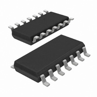
74LV27D,112 NXP Semiconductors, 74LV27D,112 Datasheet - Page 2

74LV27D,112
Manufacturer Part Number
74LV27D,112
Description
IC TRIPLE 3-IN NOR GATE 14-SOIC
Manufacturer
NXP Semiconductors
Series
74LVr
Datasheet
1.74LV27D118.pdf
(8 pages)
Specifications of 74LV27D,112
Number Of Circuits
3
Package / Case
14-SOIC (3.9mm Width), 14-SOL
Logic Type
NOR Gate
Number Of Inputs
3
Current - Output High, Low
12mA, 12mA
Voltage - Supply
1 V ~ 5.5 V
Operating Temperature
-40°C ~ 125°C
Mounting Type
Surface Mount
Product
NOR
Logic Family
LV
High Level Output Current
- 12 mA
Low Level Output Current
12 mA
Propagation Delay Time
8 ns
Supply Voltage (max)
5.5 V
Supply Voltage (min)
1 V
Maximum Operating Temperature
+ 125 C
Mounting Style
SMD/SMT
Minimum Operating Temperature
- 40 C
Lead Free Status / RoHS Status
Lead free / RoHS Compliant
Lead Free Status / RoHS Status
Lead free / RoHS Compliant, Lead free / RoHS Compliant
Other names
568-2952-5
935167470112
935167470112
1. C
2. The condition is V
Philips Semiconductors
FEATURES
QUICK REFERENCE DATA
GND = 0 V; T
NOTES:
ORDERING INFORMATION
PIN CONFIGURATION
14-Pin Plastic SO
2003 Mar 10
Wide operating voltage: 1.0 to 5.5 V
Optimized for Low Voltage applications: 1.0 to 3.6 V
Accepts TTL input levels between V
Typical V
T
Typical V
T
Output capability: standard
I
Triple 3-input NOR gate
CC
P
N = number of outputs switching;
f
f
amb
amb
i
o
PD
D
= input frequency in MHz; C
(C
= output frequency in MHz; V
category: SSI
= C
= 25 C.
= 25 C.
SYMBOL
L
t
is used to determine the dynamic power dissipation (P
PHL
C
PD
OLP
OHV
C
V
PD
/t
CC
I
amb
PLH
2
V
(output ground bounce) < 0.8 V at V
(output V
PACKAGES
GND
CC
= 25 C; t
f
2C
1A
1B
2A
2B
2Y
o
2
) = sum of the outputs.
I
= GND to V
f
i
6
2
3
4
5
7
1
OH
Propagation delay
nA, nB, nC to nY
Input capacitance
Power dissipation capacitance per gate
N +
r
= t
undershoot) > 2 V at V
f
(C
L
2.5 ns
CC.
= output load capacitance in pF;
CC
L
CC
= supply voltage in V;
V
PARAMETER
CC
= 2.7 V and V
14
13
12
10
2
11
8
9
f
o
V
1C
1Y
3C
3B
3A
3Y
) where:
CC
TEMPERATURE RANGE
CC
CC
–40 C to +125 C
= 3.3 V,
= 3.3 V,
CC
= 3.6 V
SV00446
D
in W)
C
V
See Notes 1 and 2
L
CC
2
= 15 pF;
= 3.3 V
DESCRIPTION
The 74LV27 is a low-voltage Si-gate CMOS device and is pin and
function compatible with 74HC/HCT27.
The 74LV27 provides the 3-input NOR function.
PIN DESCRIPTION
PIN NUMBER
1, 3, 9
2, 4, 10
13, 5, 11
7
12, 6, 8
14
CONDITIONS
ORDER CODE
SYMBOL
1C – 3C
1A – 3A
1B – 3B
1Y – 3Y
74LV27D
GND
V
CC
Data inputs
Data inputs
Data inputs
Ground (0 V)
Data outputs
Positive supply voltage
TYPICAL
NAME AND FUNCTION
3.5
24
8
PKG. DWG. #
SOT108-1
74LV27
Product data
UNIT
pF
pF
ns


