MC74HCT74ADR2 ON Semiconductor, MC74HCT74ADR2 Datasheet
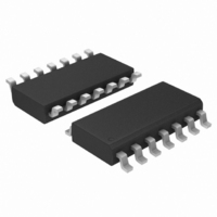
IC FLIP-FLOP DUAL SET/RST 14SOIC

MC74HCT74ADR2

Manufacturer Part Number
MC74HCT74ADR2
Description
IC FLIP-FLOP DUAL SET/RST 14SOIC
Manufacturer
ON Semiconductor
Series
74HCTr
Type
D-Typer
Datasheet

Specifications of MC74HCT74ADR2

Function
Set(Preset) and Reset
Output Type
Differential
Number Of Elements
2
Number Of Bits Per Element
1
Frequency - Clock
30MHz
Delay Time - Propagation
24ns
Trigger Type
Positive Edge
Current - Output High, Low
4mA, 4mA
Voltage - Supply
4.5 V ~ 5.5 V
Operating Temperature
-55°C ~ 125°C
Mounting Type
Surface Mount
Package / Case
14-SOIC (3.9mm Width), 14-SOL
Lead Free Status / RoHS Status
Contains lead / RoHS non-compliant
Other names
MC74HCT74ADR2OSCT

Available stocks

Company
Part Number
Manufacturer
Quantity
Price
Part Number:
MC74HCT74ADR2G
Manufacturer:
ON Semiconductor
Quantity:
3 700
Company:
Part Number:
MC74HCT74ADR2G
Quantity:
126
MC74HCT74A
Dual D Flip−Flop with Set
and Reset with LSTTL
Compatible Inputs
High−Performance Silicon−Gate CMOS
may be used as a level converter for interfacing TTL or NMOS outputs
to High Speed CMOS inputs.
and Clock inputs. Information at a D−input is transferred to the
corresponding Q output on the next positive going edge of the clock
input. Both Q and Q outputs are available from each flip−flop. The Set
and Reset inputs are asynchronous.
Features
© Semiconductor Components Industries, LLC, 2006
October, 2006 − Rev. 10
The MC74HCT74A is identical in pinout to the LS74. This device
This device consists of two D flip−flops with individual Set, Reset,
Output Drive Capability: 10 LSTTL Loads
TTL NMOS Compatible Input Levels
Outputs Directly Interface to CMOS, NMOS, and TTL
Operating Voltage Range: 4.5 to 5.5 V
Low Input Current: 1.0 mA
In Compliance With the JEDEC Standard No. 7.0 A Requirements
Chip Complexity: 136 FETs or 34 Equivalent Gates
Pb−Free Packages are Available
Î Î Î Î Î Î Î Î Î Î
Î Î Î Î Î Î Î Î Î Î
Î Î Î Î Î Î Î Î Î Î
Î Î Î Î Î Î Î Î Î Î
Î Î Î Î Î Î Î Î Î Î
Î Î Î Î Î Î Î Î Î Î
Î Î Î Î Î Î Î Î Î Î
Î Î Î Î Î Î Î Î Î Î
Î Î Î Î Î Î Î Î Î Î
Î Î Î Î Î Î Î Î Î Î
†Equivalent to a two−input NAND gate.
Internal Gate Count†
Internal Gate Propagation Delay
Internal Gate Power Dissipation
Speed Power Product
RESET 1
CLOCK 1
CLOCK 2
RESET 2
DATA 1
DATA 2
Design Criteria
SET 1
SET 2
LOGIC DIAGRAM
13
12
11
10
1
2
3
4
Î Î Î Î
Î Î Î Î
Î Î Î Î
Î Î Î Î
Î Î Î Î
Î Î Î Î
Î Î Î Î
Î Î Î Î
Î Î Î Î
Î Î Î Î
PIN 14 = V
PIN 7 = GND
5
6
9
8
Value
.0075
Q1
Q2
Q2
1.5
5.0
Q1
34
CC
Î Î Î
Î Î Î
Î Î Î
Î Î Î
Î Î Î
Î Î Î
Î Î Î
Î Î Î
Î Î Î
Î Î Î
Units
mW
ea.
ns
pJ
1
14
*Both outputs will remain high as long as Set and
See detailed ordering and shipping information in the package
dimensions section on page 3 of this data sheet.
Reset are low, but the output states are unpredict-
able if Set and Reset go high simultaneously.
14
1
Set Reset Clock Data
1
H
H
H
H
H
H
L
L
CLOCK 1
RESET 1
ORDERING INFORMATION
DATA 1
A
L, WL
Y, YY
W, WW = Work Week
G
SET 1
GND
Q1
Q1
H
H
H
H
H
H
L
L
http://onsemi.com
FUNCTION TABLE
PIN ASSIGNMENT
Inputs
CASE 751A
CASE 646
N SUFFIX
D SUFFIX
SOIC−14
PDIP−14
= Assembly Location
= Wafer Lot
= Year
= Pb−Free Package
1
2
3
4
5
6
7
X
X
X
H
L
Publication Order Number:
14
H
X
X
X
L
X
X
X
1
14
13
12
10
14
11
9
8
1
MC74HCT74AN
DIAGRAMS
MC74HCT74A/D
AWLYYWWG
V
RESET 2
DATA 2
CLOCK 2
SET 2
Q2
Q2
No Change
No Change
No Change
MARKING
H*
CC
Outputs
Q
H
H
L
L
HCT74AG
AWLYWW
H*
Q
H
H
L
L

Related parts for MC74HCT74ADR2

MC74HCT74ADR2 Summary of contents

Page 1

MC74HCT74A Dual D Flip−Flop with Set and Reset with LSTTL Compatible Inputs High−Performance Silicon−Gate CMOS The MC74HCT74A is identical in pinout to the LS74. This device may be used as a level converter for interfacing TTL or NMOS outputs to ...

Page 2

... Information on typical parametric values can be found in Chapter 2 of the ON Semiconductor High−Speed CMOS Data Book (DL129/D). Î Î Î Î Î Î Î Î ...

Page 3

... ORDERING INFORMATION Device MC74HCT74AN MC74HCT74ANG MC74HCT74AD MC74HCT74ADG MC74HCT74ADR2 MC74HCT74ADR2G †For information on tape and reel specifications, including part orientation and tape sizes, please refer to our Tape and Reel Packaging Specifications Brochure, BRD8011/ 5.0 V ± 10 pF, Input ...

Page 4

V CLOCK 1 1/f max t t PLH PHL 90 1 TLH THL Figure 1. VALID 1.3 V DATA 1.3 ...

Page 5

−T− SEATING PLANE 0.13 (0.005) PACKAGE DIMENSIONS PDIP−14 CASE 646−06 ISSUE http://onsemi.com 5 NOTES: 1. DIMENSIONING AND TOLERANCING PER ANSI ...

Page 6

... Pb−Free strategy and soldering details, please download the ON Semiconductor Soldering and Mounting Techniques Reference Manual, SOLDERRM/D. ON Semiconductor and are registered trademarks of Semiconductor Components Industries, LLC (SCILLC). SCILLC reserves the right to make changes without further notice to any products herein ...

Related keywords