74ABT74DB,112 NXP Semiconductors, 74ABT74DB,112 Datasheet - Page 3
74ABT74DB,112
Manufacturer Part Number
74ABT74DB,112
Description
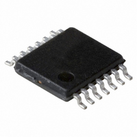
IC DUAL D-TYPE F-F 14-SSOP
Manufacturer
NXP Semiconductors
Series
74ABTr
Type
D-Typer
Datasheet
1.74ABT74D112.pdf
(5 pages)
Specifications of 74ABT74DB,112
Output Type
Differential
Package / Case
14-SSOP
Function
Set(Preset) and Reset
Number Of Elements
2
Number Of Bits Per Element
1
Frequency - Clock
250MHz
Delay Time - Propagation
3ns
Trigger Type
Positive Edge
Current - Output High, Low
15mA, 20mA
Voltage - Supply
4.5 V ~ 5.5 V
Operating Temperature
-40°C ~ 85°C
Mounting Type
Surface Mount
Number Of Circuits
2
Logic Family
ABT
Logic Type
D-Type Edge Triggered Flip-Flop
Polarity
Inverting/Non-Inverting
Input Type
Single-Ended
Propagation Delay Time
3 ns
High Level Output Current
- 15 mA
Low Level Output Current
20 mA
Supply Voltage (max)
5.5 V
Maximum Operating Temperature
+ 85 C
Mounting Style
SMD/SMT
Minimum Operating Temperature
- 40 C
Supply Voltage (min)
4.5 V
Lead Free Status / RoHS Status
Lead free / RoHS Compliant
Lead Free Status / RoHS Status
Lead free / RoHS Compliant, Lead free / RoHS Compliant
Other names
568-2492-5
935208750112
935208750112


1. Not more than one output should be tested at a time, and the duration of the test should not exceed one second.
2. This is the increase in supply current for each input at 3.4V.
3. For valid test results, data must not be loaded into the flip-flop or latch after applying the power.
1. Skew is defined as the absolute value of the difference between the actual propagation delay for any two separate outputs of the same
Philips Semiconductors
DC ELECTRICAL CHARACTERISTICS
NOTES:
AC ELECTRICAL CHARACTERISTICS
GND = 0V; t
NOTE:
AC SETUP REQUIREMENTS
GND = 0V; t
1995 Sep 22
SYMBOL
SYMBOL
SYMBOL
SYMBOL
Dual D-type flip-flop
device. The specification applies to any outputs switching in the the same direction, either HIGH–to-LOW (t
parameter guaranteed by design.
SYMBOL
SYMBOL
t
t
OSLH
V
I
I
V
f
t
t
t
t
OSHL
V
OFF
CEX
I
t
MAX
t
t
I
CC
PLH
PHL
PLH
PHL
I
t
t
t
OH
su
t
w
OL
I
su
O
CC
h
IK
h
w
w
I
t
rec
(H)
(L)
(H)
(H)
(L)
(L)
(L)
1
R
R
Input clamp voltage
High-level output voltage
Low-level output voltage
Input leakage current
Power-off leakage current
Output High leakage current
Output current
Quiescent supply current
Additional supply current per
input pin
= t
= t
Maximum clock frequency
Propagation delay
CPn to Qn, Qn
Propagation delay
Sn, Rn to Qn, Qn
Output to Output skew
An or Bn to Yn
F
F
Setup time, high or low
Dn to CPn
Hold time, high or low
Dn to CPn
CPn pulse width,
high or low
SDn, RDn pulse width, low
Recovery time
SDn, RDn to CPn
= 2.5ns; C
= 2.5ns; C
PARAMETER
PARAMETER
2
PARAMETER
PARAMETER
1
PARAMETER
PARAMETER
L
L
= 50pF, R
= 50pF, R
L
L
= 500
= 500
V
V
V
V
V
V
V
V
V
inputs at V
CC
CC
CC
CC
CC
CC
CC
CC
CC
= 4.5V; I
= 4.5V; I
= 4.5V; I
= 5.5V; V
= 0.0V; V
= 5.5V; V
= 5.5V; V
= 5.5V; V
= 5.5V; One data input at 3.4V, other
WAVEFORM
WAVEFORM
CC
TEST CONDITIONS
TEST CONDITIONS
WAVEFORM
WAVEFORM
IK
OH
OL
or GND
I
O
O
O
I
= GND or 5.5V
= GND or V
= –18mA
or V
= 5.5V; V
= 2.5V
1
1
3
4
= 20mA; V
= –15mA; V
1
1
1
3
2
I
4.5V
I
3
= GND or V
I
CC
= V
I
= V
MIN
180
IL
1.0
1.0
1.0
1.0
IL
MIN
or V
2.6
2.4
1.7
1.7
2.0
2.1
T
0
0
V
or V
amb
T
CC
V
amb
IH
CC
CC
IH
= +5.0V
= +25 C
TYP
250
= +5.0V
3.0
2.5
3.4
2.9
0.5
= +25 C
TYP
–1.4
–1.4
1.4
1.4
1.0
1.0
1.3
1.4
MIN
–50
2.5
MAX
4.2
3.5
4.9
4.5
0.6
T
LIMITS
LIMITS
amb
T
TYP
–0.9
0.35
0.25
–75
2.9
0.01
5.0
amb
= +25 C
5.0
2
V
T
CC
amb
= –40 C to +85 C
V
MIN
150
= +5.0V 0.5V
1.0
1.0
1.0
1.0
CC
LIMITS
OSHL
MAX
–180
–1.2
500
= –40 C to +85 C
0.5
MIN
100
50
50
2.6
2.4
2.1
2.1
2.2
2.4
1.0
= +5.0V 0.5V
0
0
) or LOW-to-HIGH (t
T
MIN
–50
amb
2.5
to +85 C
MAX
4.7
4.0
6.2
5.2
0.6
Product specification
74ABT74
= –40 C
MAX
–180
–1.2
500
0.5
100
50
50
1.0
UNIT
UNIT
UNIT
UNIT
MHz
ns
ns
ns
ns
ns
OSLH
ns
ns
ns
UNIT
UNIT
mA
V
V
V
A
A
A
A
A
);
Related parts for 74ABT74DB,112
Image
Part Number
Description
Manufacturer
Datasheet
Request
R

Part Number:
Description:
Flip Flops DUAL D-TYPE FLIPFLOP
Manufacturer:
NXP Semiconductors
Datasheet:

Part Number:
Description:
IC FLIP FLOP DUAL D OCTAL 14SOIC
Manufacturer:
NXP Semiconductors
Datasheet:
Part Number:
Description:
IC DUAL D-TYPE F-F 14SOIC
Manufacturer:
NXP Semiconductors
Datasheet:

Part Number:
Description:
Dual D-type Flip-flop
Manufacturer:
NXP Semiconductors
Datasheet:

Part Number:
Description:
IC TRANSCVR TRI-ST 8BIT 20SOIC
Manufacturer:
Fairchild Semiconductor
Datasheet:

Part Number:
Description:
IC BUFF/DVR TRI-ST 8BIT 20SOIC
Manufacturer:
Fairchild Semiconductor
Datasheet:
Part Number:
Description:
IC BUFF TRI-ST QD N-INV 14SOICN
Manufacturer:
NXP Semiconductors
Datasheet:
Part Number:
Description:
IC BUFF/DVR TRI-ST 8BIT 20SOIC
Manufacturer:
NXP Semiconductors
Datasheet:
Part Number:
Description:
IC BUFF/DVR TRI-ST DUAL 20SOIC
Manufacturer:
NXP Semiconductors
Datasheet:

Part Number:
Description:
IC BUFF/DVR TRI-ST DUAL 20SOIC
Manufacturer:
Fairchild Semiconductor
Datasheet:

Part Number:
Description:
IC BUFF/DVR TRI-ST 8BIT 20DIP
Manufacturer:
NXP Semiconductors
Datasheet:

Part Number:
Description:
IC BUFF TRI-ST QD N-INV 14TSSOP
Manufacturer:
Fairchild Semiconductor

Part Number:
Description:
IC BUFF TRI-ST QD N-INV 14SOIC
Manufacturer:
Fairchild Semiconductor

Part Number:
Description:
IC BUFF/DVR TRI-ST DUAL 20TSSOP
Manufacturer:
Fairchild Semiconductor
Part Number:
Description:
IC BUFF/DVR TRI-ST DUAL 20TSSOP
Manufacturer:
Fairchild Semiconductor
Datasheet: