74ALVC374BQ,115 NXP Semiconductors, 74ALVC374BQ,115 Datasheet - Page 4
74ALVC374BQ,115
Manufacturer Part Number
74ALVC374BQ,115
Description
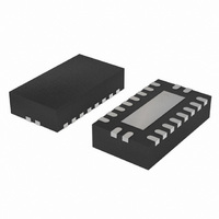
IC OCT D FF POS-EDGTRIG 20DHVQFN
Manufacturer
NXP Semiconductors
Series
74ALVCr
Type
D-Type Busr
Datasheet
1.74ALVC374BQ115.pdf
(17 pages)
Specifications of 74ALVC374BQ,115
Function
Standard
Output Type
Tri-State Non Inverted
Number Of Elements
1
Number Of Bits Per Element
8
Frequency - Clock
300MHz
Delay Time - Propagation
3.1ns
Trigger Type
Positive Edge
Current - Output High, Low
24mA, 24mA
Voltage - Supply
1.65 V ~ 3.6 V
Operating Temperature
-40°C ~ 85°C
Mounting Type
Surface Mount
Package / Case
20-VQFN Exposed Pad, 20-HVQFN, 20-SQFN, 20-DHVQFN
Lead Free Status / RoHS Status
Lead free / RoHS Compliant
Other names
74ALVC374BQ-G
74ALVC374BQ-G
935285558115
74ALVC374BQ-G
935285558115


NXP Semiconductors
5. Pinning information
Table 2.
74ALVC374_2
Product data sheet
Symbol
D[0:7]
CP
OE
Q[0:7]
V
GND
Fig 5. Pin configuration SO20 and TSSOP20
CC
Pin description
GND
OE
Q0
Q1
Q2
Q3
D0
D1
D2
D3
5.1 Pinning
5.2 Pin description
Pin
3, 4, 7, 8, 13, 14, 17, 18
11
1
2, 5, 6, 9, 12, 15, 16, 19
20
10
10
1
2
3
4
5
6
7
8
9
374
001aad040
20
19
18
17
16
15
14
13
12
11
V
Q7
D7
D6
Q6
Q5
D5
D4
Q4
CP
CC
Description
data input
clock input (LOW to HIGH, edge-triggered)
output enable input (active LOW)
3-state flip-flop output
supply voltage
ground (0 V)
Rev. 02 — 17 October 2007
Octal D-type flip-flop; positive-edge trigger; 3-state
Fig 6. Pin configuration DHVQFN20
(1) The die substrate is attached to this pad using
conductive die attach material. It can not be used as
a supply pin or input.
index area
terminal 1
Q0
D0
D1
Q1
Q2
D2
D3
Q3
Transparent top view
2
3
4
5
6
7
8
9
GND
374
(1)
74ALVC374
19
18
17
16
15
14
13
12
001aad088
© NXP B.V. 2007. All rights reserved.
Q7
D7
D6
Q6
Q5
D5
D4
Q4
4 of 17
Related parts for 74ALVC374BQ,115
Image
Part Number
Description
Manufacturer
Datasheet
Request
R

Part Number:
Description:
IC BUFF DVR 16BIT LOW V 48TSSOP
Manufacturer:
Fairchild Semiconductor
Datasheet:
Part Number:
Description:
IC BUFF DVR 16BIT LOW V 48TSSOP
Manufacturer:
Fairchild Semiconductor
Datasheet:
Part Number:
Description:
IC TRANSCVR 16BIT LOW V 48TSSOP
Manufacturer:
Fairchild Semiconductor
Datasheet:

Part Number:
Description:
IC BUFF/DVR TRI-ST DUAL 20SOIC
Manufacturer:
NXP Semiconductors
Datasheet:
Part Number:
Description:
IC BUFF/DVR TRI-ST 8BIT 20SOIC
Manufacturer:
NXP Semiconductors
Datasheet:

Part Number:
Description:
IC BUFF/DVR TRI-ST 8BIT 20TSSOP
Manufacturer:
NXP Semiconductors
Datasheet:

Part Number:
Description:
IC BUFF DVR TRI-ST 16BIT 48SSOP
Manufacturer:
NXP Semiconductors
Datasheet:
Part Number:
Description:
IC BUFF DVR TRI-ST 16BIT 48TSSOP
Manufacturer:
NXP Semiconductors
Datasheet:
Part Number:
Description:
IC TRANSCVR 3-ST 16BIT 48SSOP
Manufacturer:
NXP Semiconductors
Datasheet:
Part Number:
Description:
IC TRANSCVR TRI-ST 16BIT 48TSSOP
Manufacturer:
NXP Semiconductors
Datasheet:

Part Number:
Description:
IC TRANSCVR TRI-ST 16BIT 48TSSOP
Manufacturer:
IDT, Integrated Device Technology Inc
Datasheet:

Part Number:
Description:
IC BUFF DVR 20BIT LOW V 56TSSOP
Manufacturer:
Fairchild Semiconductor
Datasheet:
Part Number:
Description:
IC TRANSCVR 16BIT LOW V 54FBGA
Manufacturer:
Fairchild Semiconductor
Datasheet:
Part Number:
Description:
IC TRANSCVR 16BIT LOW V 48TSSOP
Manufacturer:
Fairchild Semiconductor
Datasheet:

Part Number:
Description:
IC TRANSCVR TRI-ST 8BIT 20TSSOP
Manufacturer:
Fairchild Semiconductor
Datasheet: