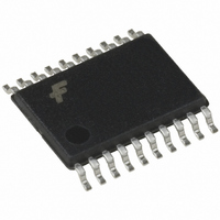
74ACT273MTC Fairchild Semiconductor, 74ACT273MTC Datasheet - Page 5

74ACT273MTC
Manufacturer Part Number
74ACT273MTC
Description
IC FLIP FLOP OCT D TYPE 20-TSSOP
Manufacturer
Fairchild Semiconductor
Series
74ACTr
Type
D-Type Busr
Datasheet
1.74ACT273MTC.pdf
(7 pages)
Specifications of 74ACT273MTC
Function
Master Reset
Output Type
Non-Inverted
Number Of Elements
1
Number Of Bits Per Element
8
Frequency - Clock
189MHz
Delay Time - Propagation
6.5ns
Trigger Type
Positive Edge
Current - Output High, Low
24mA, 24mA
Voltage - Supply
4.5 V ~ 5.5 V
Operating Temperature
-40°C ~ 85°C
Mounting Type
Surface Mount
Package / Case
20-TSSOP
Number Of Circuits
8
Logic Family
74ACT
Logic Type
D-Type Flip-Flop
Polarity
Non-Inverting
Input Type
Single-Ended
Propagation Delay Time
8.5 ns
High Level Output Current
- 24 mA
Low Level Output Current
24 mA
Supply Voltage (max)
5.5 V
Maximum Operating Temperature
+ 85 C
Mounting Style
SMD/SMT
Minimum Operating Temperature
- 40 C
Supply Voltage (min)
4.5 V
Lead Free Status / RoHS Status
Lead free / RoHS Compliant
FM3565 Rev. A.1
Supply Voltage (V
DC Input Voltage (V
Output Voltage (V
DC Input Diode Current (I
DC Output Diode Current (I
DC Output Source/Sink Current (I
DC V
Storage Temperature Range (T
parametric values defined in the “Electrical Characteristics” table are not guaranteed at the Absolute Maximum Ratings. The “Recommended Operating Conditions” table will
define the conditions for actual device operation.
Outputs 3-stated
Outputs Active (Note 2)
V
V
Supply Pin (I
CC
V
V
V
I
Floating or unused pins (inputs or I/O’s) must be held HIGH or LOW.
V
V
I
V
V
I
The “Absolute Maximum Ratings” are those values beyond which the safety of the device cannot be guaranteed. The device should not be operated at these limits. The
I
I
O
O
O
CC
CC
IR
OH
IR
OL
OL
IH
IH
IL
IL
Absolute Maximum Rating must be observed.
< 0V
> Vcc
or Ground Current per
CC
High Level Input Voltage
Low Level Input Voltage
Low Level Output Voltage
Input Leakage Current
Quiescent Supply Current
High Level Input Voltage
Low Level Input Voltage
Low Level Output Voltage
Output High Voltage
Input Leakage Current
Quiescent Supply Current
O
CC
)
I
)
or Ground)
)
IK
) V
OK
)
I
< 0V
STG
OH
)
/I
OL
)
-0.5 to V
-65
-0.5V to +6.5V
-0.5V to +6.5V
-0.5V to +6.5V
°
C to +150
±100mA
CC
≤
+50mA
±50mA
-50mA
-50mA
+0.5V
Fixed output mode, ('S' grade
I
I
V
V
V
I
I
samples, or FM3560 with
LEVEL input = logical ‘0’) 1
TTL load, 50pF capacitance
V
V
OL
OL
OL
OL
I
I
CC
I
CC
°
=V
≤
=V
= V
C
= 100µA
= 3mA
= 100µA
= 3mA
≤ (V
≤ (V
IL
IL
CC
, V
, V
I,
I,
CC
CC
or GND
≤
V
V
Power Supply
Input Voltage
Output Voltage (V
Output Current I
Free Air Operating Temperature(TA)
Minimum Input Edge Rate (dt/dv)
O
O
= 5.5V
= 5.5V
) ≤ 3.6V
) ≤ 3.6V
V
IN
= 0.8V to 2.0V, V
OL
O
)
CC
V
V
CC
CC
= 3.0V
300
300
-10
-10
2.3
x 0.7
x 0.7
V
V
CC
CC
+10
975
+10
975
0.2
0.4
0.2
0.4
2.5
x 0.3
x 0.3
www.fairchildsemi.com
www.fairchildsemi.com
-0°C to +70°C
-0.3V to 5.5V
3.0V to 5.5V
0V to V
µA
µA
µA
µA
10ns/V
V
V
V
V
V
V
V
3mA
CC


