CY7C4255-10AXC Cypress Semiconductor Corp, CY7C4255-10AXC Datasheet
CY7C4255-10AXC
Specifications of CY7C4255-10AXC
Available stocks


Related parts for CY7C4255-10AXC


CY7C4255-10AXC Summary of contents
Page 1
... FIFO on each cycle. The output port is controlled in a similar manner by a free-running Read Clock (RCLK) and a Read Enable pin (REN). In addition, the CY7C4255/65/65A have an Output Enable pin (OE). The read and write clocks may be tied together for single-clock operation or the two clocks may be run independently for asynchronous read/write applications ...
Page 2
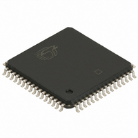
... Pin Configurations Figure 1. 64-Pin TQFP/STQFP (Top View) Pin Description The CY7C4255/65/65A provides five status pins. These pins are decoded to determine one of five states: Empty, Almost Empty, Half Full, Almost Full, and Full. The Half Full flag shares the WXO pin. This flag is valid in the standalone and width-expansion configurations ...
Page 3
... I CC Almost Empty/ Almost Full Flags Document #: 38-06004 Rev. *E CY7C4255, CY7C4265, CY7C4265A Function Data inputs for an 18-bit bus. Enables the WCLK input. Enables the RCLK input. The rising edge clocks data into the FIFO when WEN is LOW and the FIFO is not Full. ...
Page 4
... CC 8. Tested initially and after any design changes that may affect these parameters. 9. Tested initially and after any process changes that may affect these parameters. Document #: 38-06004 Rev. *E CY7C4255, CY7C4265, CY7C4265A Output Current into Outputs (LOW)............................. 20 mA [2] Static Discharge Voltage............................................ >2001V (per MIL– ...
Page 5
... CC t Clock to Programmable Almost-Full Flag PAEsynch (Synchronous mode, V /SMODE tied Clock to Half-Full Flag HF t Clock to Expansion Out XO Document #: 38-06004 Rev. *E CY7C4255, CY7C4265, CY7C4265A [10, 11] ALL INPUT PULSES 3.0V 10% GND ≤ Equivalent to: THÉ VENIN EQUIVALENT 410Ω OUTPUT 7C42X5, 7C42X5-10 7C4265A-15 ...
Page 6
... AC parameters except for t L OHZ 11 for OHZ 12. Pulse widths less than minimum values are not enabled. 13. Values guaranteed by design, not currently tested. 14 after program register write is not be valid until PAFasynch PAEasynch Document #: 38-06004 Rev. *E CY7C4255, CY7C4265, CY7C4265A 7C42X5, 7C42X5-10 7C4265A-15 Min Max Min 4.5 6 ...
Page 7
... WCLK edge and a rising RCLK edge to guarantee that EF goes HIGH during the current clock cycle. It the time SKEW2 between the rising edge of WCLK and the rising edge of RCLK is less than t Document #: 38-06004 Rev. *E CY7C4255, CY7C4265, CY7C4265A Figure 3. Write Cycle Timing t CLK ...
Page 8
... When t > minimum specification, t (maximum SKEW2 FRL The Latency Timing applies only at the Empty Boundary (EF = LOW). CLK SKEW2 20. The first word is available the cycle after EF goes HIGH, always. Document #: 38-06004 Rev. *E CY7C4255, CY7C4265, CY7C4265A [17] Figure 5. Reset Timing RSR t RSF t RSF t RSF ...
Page 9
... SKEW1 D – WFF FF WEN RCLK t ENH t ENS REN LOW DATA IN OUTPUT REGISTER Q – Document #: 38-06004 Rev. *E CY7C4255, CY7C4265, CY7C4265A Figure 7. Empty Flag Timing ENS t t REF REF t A Figure 8. Full Flag Timing [15 SKEW1 DATA WRITE t WFF t ENS DATA READ D1 t ENH ...
Page 10
... REN Figure 10. Programmable Almost Empty Flag Timing t CLKH WCLK WEN [21] PAE RCLK REN Note 21. PAE is offset = n. Number of data words into FIFO already = n. Document #: 38-06004 Rev. *E CY7C4255, CY7C4265, CY7C4265A Figure 9. Half-Full Flag Timing t CLKL t t ENS ENH t HF HALF FULL + 1 OR MORE t ...
Page 11
... If a read is preformed on this rising edge of the read clock, there are Empty + (n−1) words in the FIFO when PAE goes LOW. 25. PAF offset = m. Number of data words written into FIFO already = 8192 − for the CY7C4255 and 16384 − for the CY7C4265/65A. 26. PAF is offset = m. ...
Page 12
... RCLK and a rising WCLK edge for PAF to change state during that clock cycle. If the time between the edge of SKEW3 RCLK and the rising edge of WCLK is less than t Document #: 38-06004 Rev. *E CY7C4255, CY7C4265, CY7C4265A Note 29 t CLKL ...
Page 13
... CLKH WCLK RXO t ENS REN WXI t XIS WCLK Notes 32. Write to Last Physical Location. 33. Read from Last Physical Location. Document #: 38-06004 Rev. *E CY7C4255, CY7C4265, CY7C4265A Figure 15. Read Programmable Registers t CLKL t ENH t A UNKNOWN PAE OFFSET Figure 16. Write Expansion Out Timing Note Note 32 ...
Page 14
... The flags may change state during Retransmit as a result of the offset of the read and write pointers, but flags are valid at t 36. For the synchronous PAE and PAF flags (SMODE), an appropriate clock cycle is necessary after t Document #: 38-06004 Rev. *E CY7C4255, CY7C4265, CY7C4265A Figure 19. Read Expansion In Timing t [34, 35, 36] Figure 20 ...
Page 15
... New data is Flag Operation The CY7C4255/65/65A devices provide five flag pins to indicate the condition of the FIFO contents. Empty and Full are synchronous. PAE and PAF are synchronous if V 0–17 tied outputs after 0–17 Full Flag The Full Flag (FF) goes LOW when device is Full. Write opera- tions are inhibited whenever FF is LOW regardless of the state of WEN ...
Page 16
... Notes 38 Empty Offset (Default Values: CY7C4255/CY7C4265/65A n = 127). 39 Full Offset (Default Values: CY7C4255/CY7C4265/65A n = 127). Document #: 38-06004 Rev. *E CY7C4255, CY7C4265, CY7C4265A pointer to the first physical location of the FIFO. WCLK and RCLK may be free running but must be disabled during and t after the retransmit pulse ...
Page 17
... Width Expansion Configuration The CY7C4255/65/65A can be expanded in width to provide word widths greater than 18 in increments of 18. During width expansion mode all control line inputs are common and all flags are available. Empty (Full) flags should be created by ANDing the Empty (Full) flags of every FIFO; the PAE and PAF flags can be detected from any one device. This technique avoids reading data from, or writing data to the FIFO that is “ ...
Page 18
... Figure 22. Block Diagram of 8Kx18/16Kx18 Synchronous FIFO Memory with Programmable Flags used in Depth Expansion DATA IN(D) WRITE CLOCK(WCLK) WRITE ENABLE(WEN) RESET (RS) LOAD (LD) FF PAF FIRST LOAD (FL) Document #: 38-06004 Rev. *E CY7C4255, CY7C4265, CY7C4265A Configuration WXO RXO 7C4255 7C4265 PAF PAE WXI RXI WXO RXO ...
Page 19
... SUPPLY VOLTAGE 1.40 1.20 1. 3. 25° MHz 0.60 4.00 4.50 5.00 5.50 6.00 SUPPLY VOLTAGE (V) Document #: 38-06004 Rev. *E CY7C4255, CY7C4265, CY7C4265A Figure 23. Typical AC and DC Characteristics NORMALIZED t vs. SUPPLY A TEMPERATURE 1.60 1.40 1.20 1. 25° 0.60 −55.00 5.00 5.50 6.00 AMBIENT TEMPERATURE (° ...
Page 20
... CY7C4265–10ASC CY7C4265–10ASXC CY7C4265–10AI CY7C4265–10AXI 15 CY7C4265–15AC CY7C4265–15AXC CY7C4265-15ASC CY7C4265A–15ASI Document #: 38-06004 Rev. *E CY7C4255, CY7C4265, CY7C4265A Package Package Name Type 51-85046 64-Pin Thin Quad Flatpack 51-85046 64-Pin Thin Quad Flatpack (Pb-free) 51-85051 64-Pin Small Thin Quad Flatpack ...
Page 21
... Package Diagrams Figure 24. 64-Pin Thin Plastic Quad Flat Pack ( 1.4 mm), 51-85051 Document #: 38-06004 Rev. *E CY7C4255, CY7C4265, CY7C4265A 51-85051 *A Page [+] Feedback [+] Feedback ...
Page 22
... Package Diagrams (continued) Figure 25. 64-Pin Thin Plastic Quad Flat Pack ( 1.4 mm), 51-85046 Document #: 38-06004 Rev. *E CY7C4255, CY7C4265, CY7C4265A 51-85046-*B 51-85046-*B Page [+] Feedback [+] Feedback ...
Page 23
... Power up requirements added to Maximum Ratings Information See ECN Removed PLCC package and pruned parts from Order Information See ECN Added Pb-Free logo to top of first page Added CY7C4265-10ASXC, CY7C4265-10AXI, CY7C4265-15AXC, CY7C4255-10AXC, CY7C4255-15AXC to ordering information 12/17/08 Added CY7C4265A part Updated Ordering information table psoc.cypress.com clocks.cypress.com image ...