CY7C4231-10JC Cypress Semiconductor Corp, CY7C4231-10JC Datasheet - Page 6
CY7C4231-10JC
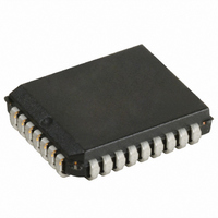
Manufacturer Part Number
CY7C4231-10JC
Description
IC SYNC FIFO MEM 2KX9 32-PLCC
Manufacturer
Cypress Semiconductor Corp
Series
CY7Cr
Datasheet
1.CY7C4211-15AXC.pdf
(18 pages)
Specifications of CY7C4231-10JC
Function
Synchronous
Memory Size
18K (2K x 9)
Data Rate
100MHz
Access Time
8ns
Voltage - Supply
3.3V
Operating Temperature
-40°C ~ 85°C
Mounting Type
Surface Mount
Package / Case
32-PLCC
Lead Free Status / RoHS Status
Contains lead / RoHS non-compliant
Other names
428-1219


Document #: 38-06016 Rev. *B
Maximum Ratings
(Above which the useful life may be impaired. For user guide-
lines, not tested.)
Storage Temperature ...................................–65
Ambient Temperature with
Power Applied...............................................–55
Supply Voltage to Ground Potential ............... –0.5V to +7.0V
DC Voltage Applied to Outputs
in High-Z State ............................................... –0.5V to +7.0V
DC Input Voltage............................................ –3.0V to +7.0V
Pin Definitions
D
Q
WEN1
WEN2/LD Dual
Mode Pin
REN1, REN2
WCLK
RCLK
EF
FF
PAE
PAF
RS
OE
Notes:
4.
5.
0–8
0–8
The Voltage on any input or I/O pin cannot exceed the power pin during power-up.
T
A
Pin
is the “instant on” case temperature.
Data Inputs
Data Outputs
Write Enable 1
Write Enable 2
Load
Read Enable
Inputs
Write Clock
Read Clock
Empty Flag
Full Flag
Programmable
Almost Empty
Programmable
Almost Full
Reset
Output Enable
Name
[4]
I/O
O Data Outputs for 9-bit Bus
O When EF is LOW, the FIFO is empty. EF is synchronized to RCLK.
O When FF is LOW, the FIFO is full. FF is synchronized to WCLK.
O When PAE is LOW, the FIFO is almost empty based on the almost empty offset value pro-
O When PAF is LOW, the FIFO is almost full based on the almost full offset value programmed into
I
I
I
I
I
I
I
I
I
Data Inputs for 9-bit Bus
The only Write enable to have programmable flags when device is configured. Data is
written on a LOW-to-HIGH transition of WCLK when WEN1 is asserted and FF is HIGH.
If the FIFO is configured to have two Write enables, data is written on a LOW-to-HIGH
transition of WCLK when WEN1 is LOW and WEN2/LD and FF are HIGH.
If HIGH at reset, this pin operates as a second Write enable. If LOW at reset, this pin
operates as a control to Write or Read the programmable flag offsets. WEN1 must be
LOW and WEN2 must be HIGH to write data into the FIFO. Data will not be written into the FIFO
if the FF is LOW. If the FIFO is configured to have programmable flags, WEN2/LD is held LOW
to write or read the programmable flag offsets.
Enables Device for Read Operation
The rising edge clocks data into the FIFO when WEN1 is LOW, WEN2/LD is HIGH, and the
FIFO is not Full. When LD is asserted, WCLK writes data into the programmable flag-offset reg-
ister.
The rising edge clocks data out of the FIFO when REN1 and REN2 are LOW and the FIFO
is not Empty. When WEN2/LD is LOW, RCLK reads data out of the programmable flag-offset
register.
grammed into the FIFO.
the FIFO.
Resets device to empty condition. A reset is required before an initial Read or Write
operation after power-up.
When OE is LOW, the FIFO’s data outputs drive the bus to which they are connected. If OE is
HIGH, the FIFO’s outputs are in High-Z (high-impedance) state.
°
°
C to +150
C to +125
°
°
C
C
Output Current into Outputs (LOW)............................. 20 mA
Static Discharge Voltage........................................... > 2001V
(per MIL-STD-883, Method 3015)
Latch-up Current..................................................... > 200 mA
Operating Range
Commercial
Industrial
Range
[5]
Description
CY7C4421/4201/4211/4221
–40
Temperature
0
CY7C4231/4241/4251
°
Ambient
C to +70
°
C to +85
°
C
°
C
Page 6 of 18
5V ±10%
5V ±10%
V
CC
Related parts for CY7C4231-10JC
Image
Part Number
Description
Manufacturer
Datasheet
Request
R

Part Number:
Description:
IC SYNC FIFO MEM 2KX9 32-PLCC
Manufacturer:
Cypress Semiconductor Corp
Datasheet:

Part Number:
Description:
Manufacturer:
Cypress Semiconductor Corp
Datasheet:

Part Number:
Description:
Manufacturer:
Cypress Semiconductor Corp
Datasheet:

Part Number:
Description:
CY7C4231-15JXCT
Manufacturer:
Cypress Semiconductor Corp
Datasheet:

Part Number:
Description:
IC,FIFO,2KX9,SYNCHRONOUS,CMOS,TQFP,32PIN,PLASTIC
Manufacturer:
Cypress Semiconductor Corp
Datasheet:
Part Number:
Description:
Manufacturer:
Cypress Semiconductor Corp
Datasheet:
Part Number:
Description:
Manufacturer:
Cypress Semiconductor Corp
Datasheet:
Part Number:
Description:
Manufacturer:
Cypress Semiconductor Corp
Datasheet: