CY7C421-20JXC Cypress Semiconductor Corp, CY7C421-20JXC Datasheet - Page 6
CY7C421-20JXC
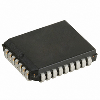
Manufacturer Part Number
CY7C421-20JXC
Description
IC ASYNC FIFO MEM 512X9 32-PLCC
Manufacturer
Cypress Semiconductor Corp
Series
CY7Cr
Specifications of CY7C421-20JXC
Access Time
10ns
Memory Size
4.6K (512 x 9)
Package / Case
32-PLCC
Function
Asynchronous
Data Rate
50MHz
Voltage - Supply
3.3V
Operating Temperature
-40°C ~ 85°C
Mounting Type
Surface Mount
Number Of Circuits
2
Data Bus Width
9 bit
Bus Direction
Unidirectional
Timing Type
Asynchronous
Organization
512 K x 9
Supply Voltage (max)
5.5 V
Supply Voltage (min)
4.5 V
Maximum Operating Current
55 mA
Maximum Operating Temperature
+ 70 C
Minimum Operating Temperature
0 C
Mounting Style
SMD/SMT
Configuration
Dual
Density
4.5Kb
Access Time (max)
20ns
Word Size
9b
Sync/async
Asynchronous
Expandable
Yes
Package Type
PLCC
Clock Freq (max)
Not RequiredMHz
Operating Supply Voltage (typ)
5V
Operating Supply Voltage (min)
4.5V
Operating Supply Voltage (max)
5.5V
Supply Current
55mA
Operating Temp Range
0C to 70C
Operating Temperature Classification
Commercial
Mounting
Surface Mount
Pin Count
32
Rohs Compliant
YES
Lead Free Status / RoHS Status
Lead free / RoHS Compliant
Lead Free Status / RoHS Status
Lead free / RoHS Compliant, Lead free / RoHS Compliant
Other names
428-2911-5
CY7C421-20JXC
CY7C421-20JXC
Available stocks
Company
Part Number
Manufacturer
Quantity
Price
Company:

Part Number:
CY7C421-20JXC
Manufacturer:
Cypress Semiconductor Corp
Quantity:
10 000
Part Number:
CY7C421-20JXC
Manufacturer:
CYPRESS/赛普拉斯
Quantity:
20 000
Company:
Part Number:
CY7C421-20JXCT
Manufacturer:
Cypress Semiconductor Corp
Quantity:
10 000


Switching Characteristics
Document #: 38-06001 Rev. *C
t
t
t
t
t
t
t
t
t
t
t
t
t
t
t
t
t
t
t
t
t
t
t
t
t
t
t
t
t
t
t
t
t
t
t
t
RC
A
RR
PR
LZR
DVR
HZR
WC
PW
HWZ
WR
SD
HD
MRSC
PMR
RMR
RPW
WPW
RTC
PRT
RTR
EFL
HFH
FFH
REF
RFF
WEF
WFF
WHF
RHF
RAE
RPE
WAF
WPF
XOL
XOH
Parameter
[6,9]
[6,9,10]
[9,10]
[6,9]
Read Cycle Time
Access Time
Read Recovery Time
Read Pulse Width
Read LOW to Low Z
Data Valid After Read HIGH
Read HIGH to High Z
Write Cycle Time
Write Pulse Width
Write HIGH to Low Z
Write Recovery Time
Data Set-Up Time
Data Hold Time
MR Cycle Time
MR Pulse Width
MR Recovery Time
Read HIGH to MR HIGH
Write HIGH to MR HIGH
Retransmit Cycle Time
Retransmit Pulse Width
Retransmit Recovery Time
MR to EF LOW
MR to HF HIGH
MR to FF HIGH
Read LOW to EF LOW
Read HIGH to FF HIGH
Write HIGH to EF HIGH
Write LOW to FF LOW
Write LOW to HF LOW
Read HIGH to HF HIGH
Effective Read from Write HIGH
Effective Read Pulse Width After EF HIGH
Effective Write from Read HIGH
Effective Write Pulse Width After FF HIGH
Expansion Out LOW Delay from Clock
Expansion Out HIGH Delay from Clock
Description
Over the Operating Range
[7, 8]
Min
40
10
30
40
30
10
18
40
30
10
30
30
40
30
10
30
30
(continued)
3
5
5
0
–30
Max
30
20
40
40
40
30
30
30
30
30
30
30
30
30
30
Min
50
10
40
50
40
10
20
50
40
10
40
40
50
40
10
40
40
3
5
5
0
–40
Max
40
20
50
50
50
35
35
35
35
35
35
35
35
40
40
CY7C419/21/25/29/33
Min
80
15
65
80
65
15
30
80
65
15
65
65
80
65
15
65
65
3
5
5
0
–65
Max
65
20
80
80
80
60
60
60
60
60
60
60
60
65
65
Page 6 of 17
Unit
ns
ns
ns
ns
ns
ns
ns
ns
ns
ns
ns
ns
ns
ns
ns
ns
ns
ns
ns
ns
ns
ns
ns
ns
ns
ns
ns
ns
ns
ns
ns
ns
ns
ns
ns
ns
[+] Feedback
Related parts for CY7C421-20JXC
Image
Part Number
Description
Manufacturer
Datasheet
Request
R

Part Number:
Description:
IC ASYNC FIFO MEM 512X9 32-PLCC
Manufacturer:
Cypress Semiconductor Corp
Datasheet:

Part Number:
Description:
IC,FIFO,512X9,ASYNCHRONOUS,CMOS,QFP,32PIN,PLASTIC
Manufacturer:
Cypress Semiconductor Corp
Datasheet:

Part Number:
Description:
Manufacturer:
Cypress Semiconductor Corp
Datasheet:
Part Number:
Description:
Manufacturer:
Cypress Semiconductor Corp
Datasheet:
Part Number:
Description:
IC ASYN FIFO MEM 512X9 32-PLCC
Manufacturer:
Cypress Semiconductor Corp
Datasheet:

Part Number:
Description:
Manufacturer:
Cypress Semiconductor Corp
Datasheet:
Part Number:
Description:
Manufacturer:
Cypress Semiconductor Corp
Datasheet:
Part Number:
Description:
Manufacturer:
Cypress Semiconductor Corp
Datasheet:
Part Number:
Description:
Manufacturer:
Cypress Semiconductor Corp
Datasheet:
Part Number:
Description:
Manufacturer:
Cypress Semiconductor Corp
Datasheet:
Part Number:
Description:
Manufacturer:
Cypress Semiconductor Corp
Datasheet:
Part Number:
Description:
Manufacturer:
Cypress Semiconductor Corp
Datasheet:
Part Number:
Description:
Manufacturer:
Cypress Semiconductor Corp
Datasheet:
Part Number:
Description:
FIFO Mem Async Dual Depth/Width Uni-Dir 512 x 9 28-Pin SOJ
Manufacturer:
Cypress Semiconductor Corp
Datasheet:
Part Number:
Description:
CY7C421-15AXCT
Manufacturer:
Cypress Semiconductor Corp
Datasheet: