MC74VHC125DG ON Semiconductor, MC74VHC125DG Datasheet
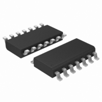
IC BUS BUFF TRI-ST QUAD 14SOIC

MC74VHC125DG

Manufacturer Part Number
MC74VHC125DG
Description
IC BUS BUFF TRI-ST QUAD 14SOIC
Manufacturer
ON Semiconductor
Series
74VHCr
Datasheet

Specifications of MC74VHC125DG

Logic Type
Buffer/Line Driver, Non-Inverting
Number Of Elements
4
Number Of Bits Per Element
1
Current - Output High, Low
8mA, 8mA
Voltage - Supply
2 V ~ 5.5 V
Operating Temperature
-55°C ~ 125°C
Mounting Type
Surface Mount
Package / Case
14-SOIC (3.9mm Width), 14-SOL
Logic Family
74VHC
Number Of Channels Per Chip
Quad
Polarity
Non-Inverting
Supply Voltage (max)
5.5 V
Supply Voltage (min)
2 V
Maximum Operating Temperature
125 C
Mounting Style
SMD/SMT
High Level Output Current
- 8 mA
Input Bias Current (max)
4 uA
Low Level Output Current
8 mA
Maximum Power Dissipation
500 mW
Minimum Operating Temperature
- 55 C
Number Of Lines (input / Output)
3
Output Type
3-State
Propagation Delay Time
11.5 ns @ 3.3 V or 7.5 ns @ 5 V
Lead Free Status / RoHS Status
Lead free / RoHS Compliant

Available stocks

Company
Part Number
Manufacturer
Quantity
Price
Part Number:
MC74VHC125DG
Manufacturer:
ON
Quantity:
20 000
MC74VHC125
Quad Bus Buffer
with 3- -State Control Inputs
fabricated with silicon gate CMOS technology. It achieves high speed
operation similar to equivalent Bipolar Schottky TTL while
maintaining CMOS low power dissipation.
High to place the output into the high impedance state.
output which provides high noise immunity and stable output. The
inputs tolerate voltages up to 7 V, allowing the interface of 5 V
systems to 3 V systems.
© Semiconductor Components Industries, LLC, 2006
March, 2006 - - Rev. 5
The MC74VHC125 is a high speed CMOS quad bus buffer
The MC74VHC125 requires the 3- -state control input (OE) to be set
The internal circuit is composed of three stages, including a buffer
These devices are available in Pb- -free package(s). Specifications herein
apply to both standard and Pb- -free devices. Please see our website at
www.onsemi.com for specific Pb- -free orderable part numbers, or
contact your local ON Semiconductor sales office or representative.
High Speed: t
Low Power Dissipation: I
High Noise Immunity: V
Power Down Protection Provided on Inputs
Balanced Propagation Delays
Designed for 2 V to 5.5 V Operating Range
Low Noise: V
Pin and Function Compatible with Other Standard Logic Families
Latchup Performance Exceeds 300 mA
ESD Performance: Human Body Model; > 2000 V,
Chip Complexity: 72 FETs or 18 Equivalent Gates
PD
OLP
= 3.8ns (Typ) at V
= 0.8 V (Max)
Machine Model; > 200 V
NIH
CC
= 4 mA (Max) at T
= V
NIL
CC
= 28% V
= 5 V
CC
A
= 25°C
1
See general marking information in the device marking
section on page 6 of this data sheet.
MC74VHC125D
MC74VHC125DT
MC74VHC125M
14- -LEAD SOIC
Device
DEVICE MARKING INFORMATION
CASE 751A
D SUFFIX
ORDERING INFORMATION
PIN CONNECTION AND
GND
OE1
OE2
MARKING DIAGRAM
A1
Y1
A2
Y2
http://onsemi.com
14- -LEAD SOIC EIAJ
(Top View)
1
2
3
4
5
6
7
CASE 965
M SUFFIX
SOIC EIAJ
Package
TSSOP
SOIC
Publication Order Number:
14
13
12
10
11
14- -LEAD TSSOP
9
8
CASE 948G
DT SUFFIX
V
OE4
A4
Y4
OE3
A3
Y3
MC74VHC125/D
CC
55 Units/Rail
96 Units/Rail
50 Units/Rail
Shipping

Related parts for MC74VHC125DG

MC74VHC125DG Summary of contents

Page 1

... These devices are available in Pb- -free package(s). Specifications herein apply to both standard and Pb- -free devices. Please see our website at www.onsemi.com for specific Pb- -free orderable part numbers, or contact your local ON Semiconductor sales office or representative. © Semiconductor Components Industries, LLC, 2006 March, 2006 - - Rev. 5 ...

Page 2

LOGIC DIAGRAM Active- -Low Output Enables OE1 OE2 OE3 OE4 FUNCTION TABLE VHC125 Inputs Output ...

Page 3

DC ELECTRICAL CHARACTERISTICS Symbol Parameter V Minimum High--Level IH Input Voltage V Maximum Low--Level IL Input Voltage V Minimum High--Level V OH Output Voltage ...

Page 4

AC ELECTRICAL CHARACTERISTICS Symbol Parameter t , Maximum Propagation Delay, PLH PHL t , Maximum Output Enable TIme, PZL PZH t , Maximum Output Disable Time, PLZ PHZ ...

Page 5

A t PLH 50 Figure 1. TEST POINT OUTPUT DEVICE UNDER C * TEST L *Includes all probe and jig capacitance Figure 3. Test Circuit INPUT SWITCHING WAVEFORMS GND t PHL Y Y ...

Page 6

MARKING DIAGRAMS VHC125 AWLYWW 14- -LEAD SOIC D SUFFIX CASE 751A *See Applications Note AND8004/D for date code and traceability information. (Top View) 14 ...

Page 7

SEATING 14 PL PLANE 0.25 (0.010 14X REF 0.10 (0.004) 0.15 (0.006 L PIN ...

Page 8

... DETAIL P VIEW American Technical Support: 800--282--9855 Toll Free USA/Canada Japan: ON Semiconductor, Japan Customer Focus Center 2--9--1 Kamimeguro, Meguro--ku, Tokyo, Japan 153--0051 Phone: 81--3--5773--3850 http://onsemi.com 8 NOTES: 1. DIMENSIONING AND TOLERANCING PER ANSI Y14.5M, 1982. 2. CONTROLLING DIMENSION: MILLIMETER. ...

Related keywords