74LCX16245MEA Fairchild Semiconductor, 74LCX16245MEA Datasheet

IC TXRX BIRDIR 16BIT 5V 48SSOP

74LCX16245MEA

Manufacturer Part Number
74LCX16245MEA
Description
IC TXRX BIRDIR 16BIT 5V 48SSOP
Manufacturer
Fairchild Semiconductor
Series
74LCXr
Datasheet

Specifications of 74LCX16245MEA

Logic Type
Transceiver, Non-Inverting
Number Of Elements
2
Number Of Bits Per Element
8
Current - Output High, Low
24mA, 24mA
Voltage - Supply
2 V ~ 3.6 V
Operating Temperature
-40°C ~ 85°C
Mounting Type
Surface Mount
Package / Case
48-SSOP
Lead Free Status / RoHS Status
Lead free / RoHS Compliant

Available stocks

Company
Part Number
Manufacturer
Quantity
Price
Part Number:
74LCX16245MEA
Manufacturer:
NS/国半
Quantity:
20 000
Part Number:
74LCX16245MEA
Quantity:
145
© 2005 Fairchild Semiconductor Corporation
74LCX16245G
(Note 2)(Note 3)
74LCX16245MEA
(Note 3)
74LCX16245MTD
(Note 3)
74LCX16245
Low Voltage 16-Bit Bidirectional Transceiver
with 5V Tolerant Inputs and Outputs
General Description
The LCX16245 contains sixteen non-inverting bidirectional
buffers with 3-STATE outputs and is intended for bus ori-
ented applications. The device is designed for low voltage
(2.5V or 3.3V) V
ing to a 5V signal environment. The device is byte con-
trolled. Each byte has separate control inputs which could
be shorted together for full 16-bit operation. The T/R inputs
determine the direction of data flow through the device.
The OE inputs disable both the A and B ports by placing
them in a high impedance state.
The LCX16245 is fabricated with an advanced CMOS tech-
nology to achieve high speed operation while maintaining
CMOS low power dissipation.
Ordering Code:
Note 2: Ordering code “G” indicates Trays.
Note 3: Devices also available in Tape and Reel. Specify by appending the suffix letter “X” to the ordering code.
Logic Symbol
Order Number
CC
Package Number
applications with capability of interfac-
BGA54A
MS48A
MTD48
54-Ball Fine-Pitch Ball Grid Array (FBGA), JEDEC MO-205, 5.5mm Wide
48-Lead Small Shrink Outline Package (SSOP), JEDEC MO-118, 0.300" Wide
48-Lead Thin Shrink Small Outline Package (TSSOP), JEDEC MO-153, 6.1mm Wide
DS012001
Features
Note 1: To ensure the high-impedance state during power up or down, OE
should be tied to V
resistor is determined by the current-sourcing capability of the driver.
5V tolerant inputs and outputs
2.3V–3.6V V
4.5 ns t
Power down high impedance inputs and outputs
Supports live insertion/withdrawal (Note 1)
r
Uses patented noise/EMI reduction circuitry
Latch-up performance exceeds 500 mA
ESD performance:
Also packaged in plastic Fine-Pitch Ball Grid Array
(FBGA)
24 mA output drive (V
Human body model
Machine model
Package Description
PD
max (V
CC
CC
through a pull-up resistor: the minimum value or the
specifications provided
CC
!
200V
!
3.3V), 20
CC
2000V
3.0V)
February 1994
Revised May 2005
P
A I
CC
www.fairchildsemi.com
max

Related parts for 74LCX16245MEA

74LCX16245MEA Summary of contents

Page 1

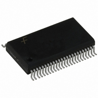
... Order Number Package Number 74LCX16245G BGA54A 54-Ball Fine-Pitch Ball Grid Array (FBGA), JEDEC MO-205, 5.5mm Wide (Note 2)(Note 3) 74LCX16245MEA MS48A 48-Lead Small Shrink Outline Package (SSOP), JEDEC MO-118, 0.300" Wide (Note 3) 74LCX16245MTD MTD48 48-Lead Thin Shrink Small Outline Package (TSSOP), JEDEC MO-153, 6.1mm Wide (Note 3) Note 2: Ordering code “ ...

Page 2

Connection Diagrams Pin Assignment for SSOP and TSSOP Pin Assignment for FBGA (Top Thru View) Logic Diagrams Note: Please note that these diagrams are provided only for the understanding of logic operations and should not be used to estimate propagation ...

Page 3

Absolute Maximum Ratings Symbol Parameter V Supply Voltage Input Voltage Output Voltage Input Diode Current Output Diode Current Output Source/Sink Current Supply ...

Page 4

DC Electrical Characteristics Symbol Parameter I Quiescent Supply Current Increase in I per Input CC CC Note 7: Outputs disabled or 3-STATE only. AC Electrical Characteristics Symbol Parameter t Propagation Delay PHL ...

Page 5

AC LOADING and WAVEFORMS FIGURE 1. AC Test Circuit (C t PLH t PZL t PZH Waveform for Inverting and Non-Inverting Functions Propagation Delay. Pulse Width and t rec 3-STATE Output Low Enable and Disable Times for Logic (Input Characteristics; ...

Page 6

Schematic Diagram Generic for LCX Family www.fairchildsemi.com 6 ...

Page 7

Physical Dimensions inches (millimeters) unless otherwise noted 54-Ball Fine-Pitch Ball Grid Array (FBGA), JEDEC MO-205, 5.5mm Wide Package Number BGA54A 7 www.fairchildsemi.com ...

Page 8

Physical Dimensions inches (millimeters) unless otherwise noted (Continued) 48-Lead Small Shrink Outline Package (SSOP), JEDEC MO-118, 0.300" Wide www.fairchildsemi.com Package Number MS48A 8 ...

Page 9

Physical Dimensions inches (millimeters) unless otherwise noted (Continued) 48-Lead Thin Shrink Small Outline Package (TSSOP), JEDEC MO-153, 6.1mm Wide Fairchild does not assume any responsibility for use of any circuitry described, no circuit patent licenses are implied and Fairchild reserves ...

Related keywords