74VCXH245MNR2G ON Semiconductor, 74VCXH245MNR2G Datasheet - Page 5
74VCXH245MNR2G
Manufacturer Part Number
74VCXH245MNR2G
Description
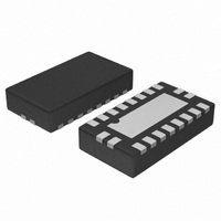
IC TXRX 8BIT 3STATE BIDIR 20QFN
Manufacturer
ON Semiconductor
Series
74VCXHr
Datasheet
1.74VCXH245MNR2G.pdf
(8 pages)
Specifications of 74VCXH245MNR2G
Logic Type
Transceiver, Non-Inverting
Number Of Elements
1
Number Of Bits Per Element
8
Current - Output High, Low
24mA, 24mA
Voltage - Supply
1.65 V ~ 3.6 V
Operating Temperature
-40°C ~ 85°C
Mounting Type
Surface Mount
Package / Case
20-TFQFN Exposed Pad
Lead Free Status / RoHS Status
Lead free / RoHS Compliant
Other names
74VCXH245MNR2GOS
74VCXH245MNR2GOS
74VCXH245MNR2GOSTR
74VCXH245MNR2GOS
74VCXH245MNR2GOSTR
Available stocks
Company
Part Number
Manufacturer
Quantity
Price
Company:

Part Number:
74VCXH245MNR2G
Manufacturer:
ON
Quantity:
42 000
Company:
Part Number:
74VCXH245MNR2G
Manufacturer:
BROADCOM
Quantity:
30


7. For C
8. Skew is defined as the absolute value of the difference between the actual propagation delay for any two separate outputs of the same device.
9. Number of outputs defined as “n”. Measured with “n−1” outputs switching from HIGH−to−LOW or LOW−to−HIGH. The remaining output is
10. Number of outputs defined as “n”. Measured with “n−1” outputs switching from HIGH−to−LOW or LOW−to−HIGH. The remaining output is
11. V
AC CHARACTERISTICS (Note 7; t
DYNAMIC SWITCHING CHARACTERISTICS
CAPACITIVE CHARACTERISTICS
Symbol
Symbol
Symbol
The specification applies to any outputs switching in the same direction, either HIGH−to−LOW (t
guaranteed by design.
measured in the LOW state.
measured in the HIGH state.
t
t
V
V
V
OSHL
OSLH
t
t
t
t
t
t
C
CC
PZH
PHZ
PLH
PHL
PZL
PLZ
C
OHV
OLP
OLV
C
OUT
PD
IN
= 1.8, 2.5 or 3.3 V; V
L
= 50 pF, add approximately 300 ps to the AC maximum specification.
Propagation Delay
Input to Output
Output Enable Time to
High and Low Level
Output Disable Time From
High and Low Level
Output−to−Output Skew
(Note 8)
Dynamic LOW Peak Voltage
(N
(Note 9)
Dynamic LOW Valley Voltage
(N
(Note 9)
Dynamic HIGH Valley Voltage
(N
(Note 10)
Input Capacitance
Output Capacitance
Power Dissipation Capacitance
Characteristic
)
)
)
Parameter
I
= 0 V or V
Parameter
CC
R
.
= t
F
Waveform
= 2.0 ns; C
1
2
2
V
V
V
V
V
V
V
V
V
CC
CC
CC
CC
CC
CC
CC
CC
CC
= 1.8 V, C
= 2.5 V, C
= 3.3 V, C
= 1.8 V, C
= 2.5 V, C
= 3.3 V, C
= 1.8 V, C
= 2.5 V, C
= 3.3 V, C
http://onsemi.com
L
V
74VCXH245
CC
= 30 pF; R
Min
0.6
0.6
0.6
0.6
0.6
0.6
= 3.0 V to 3.6 V
L
L
L
L
L
L
L
L
L
= 30 pF, V
= 30 pF, V
= 30 pF, V
= 30 pF, V
= 30 pF, V
= 30 pF, V
= 30 pF, V
= 30 pF, V
5
= 30 pF, V
Condition
Note 11, 10 MHz
Max
L
3.5
3.5
4.5
4.5
3.6
3.6
0.5
0.5
= 500 W)
Condition
Note 11
Note 11
IH
IH
IH
IH
IH
IH
IH
IH
IH
= V
= V
= V
= V
= V
= V
= V
= V
= V
V
T
CC
A
CC
CC
CC
CC
CC
CC
CC
CC
Min
CC
0.8
0.8
0.8
0.8
0.8
0.8
= −40 C to +85 C
= 2.3 V to 2.7 V
, V
, V
, V
, V
, V
, V
, V
, V
, V
IL
IL
IL
IL
IL
IL
IL
IL
Limits
IL
= 0 V
= 0 V
= 0 V
= 0 V
= 0 V
= 0 V
= 0 V
= 0 V
= 0 V
Max
OSHL
4.2
4.2
5.6
5.6
4.0
4.0
0.5
0.5
) or LOW−to−HIGH (t
V
CC
Min
1.5
1.5
1.5
1.5
1.5
1.5
= 1.65 V to1.95 V
T
A
Typical
= +25 C
−0.3
−0.7
−1.0
Typ
0.3
0.7
1.0
1.3
1.7
2.0
20
6
7
Max
0.75
0.75
8.4
8.4
9.8
9.8
7.2
7.2
OSLH
); parameter
Unit
Unit
Unit
pF
pF
pF
ns
ns
ns
ns
V
V
V
Related parts for 74VCXH245MNR2G
Image
Part Number
Description
Manufacturer
Datasheet
Request
R

Part Number:
Description:
IC TXRX 16BIT CMOS BIDIR 48TSSOP
Manufacturer:
ON Semiconductor
Datasheet:

Part Number:
Description:
IC TXRX 8BIT 3STATE BIDIR 20QFN
Manufacturer:
ON Semiconductor
Datasheet:

Part Number:
Description:
IC FLIP FLOP 16BIT D LV 48TSSOP
Manufacturer:
Fairchild Semiconductor
Datasheet:
Part Number:
Description:
IC LATCH TRANSP 16BIT LV 48TSSOP
Manufacturer:
Fairchild Semiconductor
Datasheet:

Part Number:
Description:
IC TRANS DUAL 16BIT RES 42TFBGA
Manufacturer:
STMicroelectronics
Datasheet:

Part Number:
Description:
IC TRANS DUAL 16BIT RES 48TSSOP
Manufacturer:
STMicroelectronics
Datasheet:
Part Number:
Description:
IC TXRX LEVEL TRANSLATOR 48TSSOP
Manufacturer:
STMicroelectronics
Datasheet:
Part Number:
Description:
IC TXRX LEVEL TRANSLATOR 48TSSOP
Manufacturer:
STMicroelectronics
Datasheet:
Part Number:
Description:
IC BUS BUFF TRI-ST 16BIT 48TSSOP
Manufacturer:
STMicroelectronics
Datasheet:
Part Number:
Description:
IC BUS TXRX 16BIT LV 48-TSSOP
Manufacturer:
STMicroelectronics
Datasheet:
Part Number:
Description:
IC BUFF DVR 16BIT LOW V 48TSSOP
Manufacturer:
Fairchild Semiconductor
Datasheet:
Part Number:
Description:
IC BUFF DVR 16BIT LOW V 48TSSOP
Manufacturer:
Fairchild Semiconductor
Datasheet:
Part Number:
Description:
IC BUFF DVR 16BIT LOW V 48TSSOP
Manufacturer:
Fairchild Semiconductor
Datasheet:
Part Number:
Description:
IC BUFF DVR 16BIT LOW V 48TSSOP
Manufacturer:
Fairchild Semiconductor
Datasheet:

Part Number:
Description:
TXRX BIDIRECT LOW VOLT 20TSSOP
Manufacturer:
Fairchild Semiconductor
Datasheet: