MC74ACT244NG ON Semiconductor, MC74ACT244NG Datasheet - Page 4
MC74ACT244NG
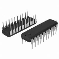
Manufacturer Part Number
MC74ACT244NG
Description
IC BUFF/DVR TRI-ST DUAL 20DIP
Manufacturer
ON Semiconductor
Series
74ACTr
Specifications of MC74ACT244NG
Logic Type
Buffer/Line Driver, Non-Inverting
Number Of Elements
2
Number Of Bits Per Element
4
Current - Output High, Low
24mA, 24mA
Voltage - Supply
4.5 V ~ 5.5 V
Operating Temperature
-40°C ~ 85°C
Mounting Type
Through Hole
Package / Case
20-DIP (0.300", 7.62mm)
Current, Supply
80 μA
Function Type
8-Channels
Logic Function
Buffer/Driver
Number Of Circuits
Octal
Package Type
PDIP-20
Special Features
Tri-State
Temperature, Operating, Range
-40 to +85 °C
Voltage, Supply
5 V
Logic Family
ACT
Number Of Channels Per Chip
8
Polarity
Non-Inverting
Supply Voltage (max)
5.5 V
Supply Voltage (min)
4.5 V
Maximum Operating Temperature
+ 85 C
Mounting Style
Through Hole
High Level Output Current
- 24 mA
Low Level Output Current
24 mA
Maximum Power Dissipation
200 mW
Minimum Operating Temperature
- 40 C
Number Of Lines (input / Output)
8 / 3
Output Type
3-State
Propagation Delay Time
9 ns at 5 V
Logic Device Type
Buffer/Line Driver, Non Inverting
Supply Voltage Range
4.5V To 5.5V
Logic Case Style
DIP
No. Of Pins
20
Operating Temperature Range
-40°C To +85°C
Filter Terminals
DIP
Rohs Compliant
Yes
Family Type
ACT
Lead Free Status / RoHS Status
Lead free / RoHS Compliant
Other names
MC74ACT244NGOS


*All outputs loaded; thresholds on input associated with output under test.
†Maximum test duration 2.0 ms, one output loaded at a time.
*Voltage Range 5.0 V is 5.0 V ±0.5 V.
DC CHARACTERISTICS
AC CHARACTERISTICS
CAPACITANCE
Symbol
Symbol
Symbol
DI
I
V
I
t
t
V
t
t
t
t
C
V
OHD
I
C
V
I
OLD
PLH
PHL
PZH
PHZ
PZL
PLZ
I
OZ
CC
CCT
OH
IN
OL
PD
IH
IN
IL
†Minimum Dynamic Output Current
Minimum High Level Input Voltage
Maximum Low Level Input Voltage
Minimum High Level Output Voltage
Maximum Low Level Output Voltage
Maximum Input Leakage Current
Additional Max. I
Maximum 3−State Current
Maximum Quiescent Supply Current
Propagation Delay
Data to Output
Propagation Delay
Data to Output
Output Enable Time
Output Enable Time
Output Disable Time
Output Disable Time
Input Capacitance
Power Dissipation Capacitance
Parameter
Parameter
(For Figures and Waveforms − See AND8277/D at www.onsemi.com)
CC
/Input
Parameter
V
(V)
5.0
5.0
5.0
5.0
5.0
5.0
CC
*
MC74AC244, MC74ACT244
Min
2.0
2.0
1.5
2.0
2.0
2.5
V
(V)
4.5
5.5
4.5
5.5
4.5
5.5
4.5
5.5
4.5
5.5
4.5
5.5
5.5
5.5
5.5
5.5
5.5
5.5
http://onsemi.com
CC
T
C
0.001
0.001
A
4.49
5.49
Typ
L
T
1.5
1.5
1.5
1.5
0.6
74ACT
−
−
−
−
−
−
−
−
−
= +25°C
4
A
= 50 pF
Typ
6.5
7.0
6.0
7.0
7.0
7.5
74ACT
= +25°C
3.86
4.86
0.36
0.36
±0.1
±0.5
2.0
2.0
0.8
0.8
4.4
5.4
0.1
0.1
8.0
−
−
−
Guaranteed Limits
Max
10.0
Value Typ
9.0
9.0
8.5
9.5
9.5
−40°C to +85°C
4.5
45
74ACT
T
3.76
4.76
0.44
0.44
±1.0
±5.0
−75
2.0
2.0
0.8
0.8
4.4
5.4
0.1
0.1
1.5
75
80
A
T
=
A
Min
1.5
1.5
1.0
1.5
1.5
2.0
= −40°C to +85°C
C
L
74ACT
= 50 pF
Unit
pF
pF
Unit
mA
mA
mA
mA
mA
mA
Max
10.0
10.0
10.5
10.5
10.5
V
V
V
V
V
V
9.5
V
or V
V
or V
I
*V
I
I
*V
I
V
V
V
V
V
V
V
V
Test Conditions
OUT
OH
OUT
OL
OUT
OUT
I
I
I
I
O
OLD
OHD
IN
IN
IN
(OE) = V
= V
= V
= V
V
V
= V
Unit
= V
CC
CC
CC
CC
= V
= V
ns
ns
ns
ns
ns
ns
Conditions
= −50 mA
= 50 mA
= 0.1 V
= 0.1 V
= 1.65 V Max
CC
CC
CC
= 3.85 V Min
CC
= 5.0 V
= 5.0 V
− 0.1 V
− 0.1 V
CC
IL
IL
, GND
, GND
− 2.1 V
, GND
or V
or V
or GND
IL
, V
−24 mA
−24 mA
24 mA
24 mA
Figure
IH
IH
IH
3−5
3−5
3−7
3−8
3−7
3−8
No.
Related parts for MC74ACT244NG
Image
Part Number
Description
Manufacturer
Datasheet
Request
R

Part Number:
Description:
ON Semiconductor [VOLTAGE REGULATOR]
Manufacturer:
ON Semiconductor
Datasheet:
Part Number:
Description:
357-036-542-201 CARDEDGE 36POS DL .156 BLK LOPRO
Manufacturer:
ON Semiconductor
Datasheet:
Part Number:
Description:
357-036-542-201 CARDEDGE 36POS DL .156 BLK LOPRO
Manufacturer:
ON Semiconductor
Datasheet:
Part Number:
Description:
357-036-542-201 CARDEDGE 36POS DL .156 BLK LOPRO
Manufacturer:
ON Semiconductor
Datasheet:
Part Number:
Description:
357-036-542-201 CARDEDGE 36POS DL .156 BLK LOPRO
Manufacturer:
ON Semiconductor
Datasheet:
Part Number:
Description:
357-036-542-201 CARDEDGE 36POS DL .156 BLK LOPRO
Manufacturer:
ON Semiconductor
Datasheet:
Part Number:
Description:
357-036-542-201 CARDEDGE 36POS DL .156 BLK LOPRO
Manufacturer:
ON Semiconductor
Datasheet:
Part Number:
Description:
357-036-542-201 CARDEDGE 36POS DL .156 BLK LOPRO
Manufacturer:
ON Semiconductor
Datasheet:
Part Number:
Description:
357-036-542-201 CARDEDGE 36POS DL .156 BLK LOPRO
Manufacturer:
ON Semiconductor
Datasheet:
Part Number:
Description:
357-036-542-201 CARDEDGE 36POS DL .156 BLK LOPRO
Manufacturer:
ON Semiconductor
Datasheet:
Part Number:
Description:
357-036-542-201 CARDEDGE 36POS DL .156 BLK LOPRO
Manufacturer:
ON Semiconductor
Datasheet:
Part Number:
Description:
Manufacturer:
ON Semiconductor
Datasheet:
Part Number:
Description:
Manufacturer:
ON Semiconductor
Datasheet:
Part Number:
Description:
Manufacturer:
ON Semiconductor
Datasheet: