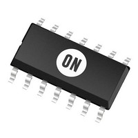
MC74VHC50MG ON Semiconductor, MC74VHC50MG Datasheet - Page 2

MC74VHC50MG
Manufacturer Part Number
MC74VHC50MG
Description
IC BUFFER HEX NON-INV 14SOEIAJ
Manufacturer
ON Semiconductor
Series
74VHCr
Datasheet
1.MC74VHC50DTR2G.pdf
(7 pages)
Specifications of MC74VHC50MG
Logic Type
Buffer/Line Driver, Non-Inverting
Number Of Elements
6
Number Of Bits Per Element
1
Current - Output High, Low
8mA, 8mA
Voltage - Supply
2 V ~ 5.5 V
Operating Temperature
-55°C ~ 125°C
Mounting Type
Surface Mount
Package / Case
14-SOIC (5.3mm Width), 14-SOP, 14-SOIJ
Logic Family
VHC
Number Of Channels Per Chip
5
Polarity
Non-Inverting
Supply Voltage (max)
5.5 V
Supply Voltage (min)
2 V
Maximum Operating Temperature
+ 125 C
Mounting Style
SMD/SMT
High Level Output Current
- 8 mA
Low Level Output Current
8 mA
Minimum Operating Temperature
- 55 C
Number Of Lines (input / Output)
6 / 3
Propagation Delay Time
10.6 ns at 3 V, 7.5 ns at 5 V
Lead Free Status / RoHS Status
Lead free / RoHS Compliant
Stresses exceeding Maximum Ratings may damage the device. Maximum Ratings are stress ratings only. Functional operation above the
Recommended Operating Conditions is not implied. Extended exposure to stresses above the Recommended Operating Conditions may affect
device reliability.
1. Measured with minimum pad spacing on an FR4 board, using 10 mm--by--1 inch, 2--ounce copper trace with no air flow.
2. Tested to EIA/JESD22--A114--A.
3. Tested to EIA/JESD22--A115--A.
4. Tested to JESD22--C101--A.
5. Tested to EIA/JESD78.
6. Unused inputs may not be left open. All inputs must be tied to a high-- or low--logic input voltage level.
NOTE:
RECOMMENDED OPERATING CONDITIONS
MAXIMUM RATINGS
V
V
V
I
I
I
I
T
T
T
θ
MSL
F
V
I
V
V
V
T
Δt/ΔV
Symbol
Symbol
IK
OK
OUT
CC
Latch--Up
JA
A
STG
L
J
R
CC
IN
OUT
ESD
CC
I
O
The θ
and figure below.
DC Supply Voltage
DC Input Voltage
DC Output Voltage
DC Input Diode Current
DC Output Diode Current
DC Output Sink Current
DC Supply Current per Supply Pin
Storage Temperature Range
Lead Temperature, 1 mm from Case for 10 Seconds
Junction Temperature under Bias
Thermal Resistance
Moisture Sensitivity
Flammability Rating
ESD Withstand Voltage
Latch--Up Performance
Supply Voltage
Input Voltage
Output Voltage
Operating Free--Air Temperature
Input Transition Rise or Fall Rate
JA
of the package is equal to 1/Derating. Higher junction temperatures may affect the expected lifetime of the device per the table
Parameter
Parameter
Above V
http://onsemi.com
CC
and Below GND at 85°C (Note 5)
Charged Device Model (Note 4)
Human Body Model (Note 2)
2
Machine Model (Note 3)
Oxygen Index: 30 to 35
(HIGH or LOW State)
V
V
CC
CC
= 3.0 V ±0.3 V
= 5.0 V ±0.5 V
V
V
O
(Note 6)
I
(Note 1)
TSSOP
< GND
< GND
SOIC
UL 94 V--0 @ 0.125 in
−55
Min
−0.5 to V
2.0
0
0
0
0
−0.5 to +7.0
−0.5 to +7.0
−65 to +150
Level 1
> 2000
Value
+150
±300
> 200
2000
−20
±20
±25
±50
260
125
170
CC
+0.5
+125
Max
V
100
5.5
5.5
20
CC
°C/W
ns/V
Unit
Unit
mA
mA
mA
mA
mA
°C
°C
°C
°C
V
V
V
V
V
V
V


