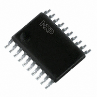
74ALVC541PW,112 NXP Semiconductors, 74ALVC541PW,112 Datasheet - Page 7

74ALVC541PW,112
Manufacturer Part Number
74ALVC541PW,112
Description
IC BUFF/DVR TRI-ST 8BIT 20TSSOP
Manufacturer
NXP Semiconductors
Series
74ALVCr
Datasheet
1.74ALVC541BQ115.pdf
(15 pages)
Specifications of 74ALVC541PW,112
Logic Type
Buffer/Line Driver, Non-Inverting
Number Of Elements
1
Number Of Bits Per Element
8
Current - Output High, Low
24mA, 24mA
Voltage - Supply
1.65 V ~ 3.6 V
Operating Temperature
-40°C ~ 85°C
Mounting Type
Surface Mount
Package / Case
20-TSSOP
Lead Free Status / RoHS Status
Lead free / RoHS Compliant
Other names
74ALVC541PW
74ALVC541PW
935269735112
74ALVC541PW
935269735112
NXP Semiconductors
Table 7.
Voltages are referenced to GND (ground = 0 V); for test circuit see
[1]
[2]
[3]
11. Waveforms
74ALVC541_2
Product data sheet
Symbol
C
Fig 5. Propagation delay input (An) to output (Yn)
PD
All typical values are measured at T
t
t
t
C
P
f
f
C
V
N = number of inputs switching;
pd
en
dis
i
o
(C
D
CC
PD
= input frequency in MHz;
L
= output frequency in MHz;
is the same as t
is the same as t
= output load capacitance in pF;
is the same as t
= C
L
is used to determine the dynamic power dissipation (P
= supply voltage in V;
Measurement points are given in
V
PD
V
OL
Dynamic characteristics
CC
Parameter
power
dissipation
capacitance
and V
2
V
CC
f
o
2
OH
) = sum of the outputs.
PLH
PZL
f
are typical voltage output levels that occur with the output load.
PLZ
i
and t
N + (C
and t
and t
PZH
PHL
PHZ
L
Conditions
per buffer; V
outputs enabled
outputs disabled
.
.
.
V
CC
amb
Yn output
An input
2
…continued
Table
= 25 C and V
f
o
) where:
I
8.
= GND to V
GND
V
V
OH
OL
V
Rev. 02 — 5 November 2007
I
CC
= 1.8 V, 2.5 V, 2.7 V and 3.3 V.
D
CC
in W).
; V
V
M
CC
V
M
t
PHL
= 3.3 V
Figure
7.
[3]
mna901
t
Min
PLH
-
-
Octal buffer/line driver; 3-state
40 C to +85 C
Typ
25
0
74ALVC541
[1]
© NXP B.V. 2007. All rights reserved.
Max
-
-
7 of 15
Unit
pF
pF


