74LCX646MTCX Fairchild Semiconductor, 74LCX646MTCX Datasheet

IC TRANSCVR/REGISTER 8B 24TSSOP

74LCX646MTCX

Manufacturer Part Number
74LCX646MTCX
Description
IC TRANSCVR/REGISTER 8B 24TSSOP
Manufacturer
Fairchild Semiconductor
Series
74LCXr
Datasheet

Specifications of 74LCX646MTCX

Logic Type
Registered Transceiver, Non-Inverting
Number Of Elements
1
Number Of Bits Per Element
8
Current - Output High, Low
24mA, 24mA
Voltage - Supply
2 V ~ 3.6 V
Operating Temperature
-40°C ~ 85°C
Mounting Type
Surface Mount
Package / Case
24-TSSOP
Lead Free Status / RoHS Status
Lead free / RoHS Compliant
© 2001 Fairchild Semiconductor Corporation
74LCX646WM
74LCX646MSA
74LCX646MTC
74LCX646
Low Voltage Octal Transceiver/Register
with 5V Tolerant Inputs and Outputs
General Description
The LCX646 consists of registered bus transceiver circuits,
D-type flip-flops, and control circuitry providing multiplexed
transmission of data directly from the input bus or from the
internal storage registers. Data on the A or B bus will be
loaded into the respective registers on the LOW-to-HIGH
transition of the appropriate pin (CPAB or CPBA) (see
Functional Description).
The LCX646 is designed for low voltage (2.5V or 3.3V) V
applications with capability of interfacing to a 5V signal
environment.
The LCX646 is fabricated with an advanced CMOS tech-
nology to achieve high speed operation while maintaining
CMOS low power dissipation.
Ordering Code:
Devices also available in Tape and Reel. Specify by appending the suffix letter “X” to the ordering code.
Connection Diagram
Order Number
Package Number
MSA24
MTC24
M24B
24-Lead Small Outline Integrated Circuit (SOIC), JEDEC MS-013, 0.300 Wide
24-Lead Shrink Small Outline Package (SSOP), EIAJ TYPE II, 5.3mm Wide
24-Lead Thin Shrink Small Outline Package (TSSOP), JEDEC MO-153, 4.4mm Wide
DS011997
CC
Features
Note 1: To ensure the high-impedance state during power up or down, OE
should be tied to V
resistor is determined by the current-sourcing capability of the driver.
Pin Descriptions
5V tolerant inputs and outputs
2.3V
7.0 ns t
Power down high impedance inputs and outputs
Supports live insertion/withdrawal (Note 1)
Implements patented noise/EMI reduction circuitry
Latch-up performance exceeds 500 mA
ESD performance:
24 mA output drive (V
Human body model
Machine model
A
B
CPAB, CPBA
SAB, SBA
OE
DIR
Package Description
0
0
–A
–B
Pin Names
3.6V V
PD
7
7
max (V
CC
CC
through a pull-up resistor: the minimum value or the
specifications provided
CC
200V
3.3V), 10 A I
Data Register A Inputs
Data Register A Outputs
Data Register B Inputs
Data Register B Outputs
Clock Pulse Inputs
Transmit/Receive Inputs
Output Enable Input
Direction Control Input
CC
2000V
3.0V)
February 1994
Revised March 2001
Description
CC
www.fairchildsemi.com
max

Related parts for 74LCX646MTCX

74LCX646MTCX Summary of contents

Page 1

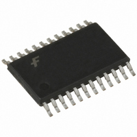
... MTC24 24-Lead Thin Shrink Small Outline Package (TSSOP), JEDEC MO-153, 4.4mm Wide Devices also available in Tape and Reel. Specify by appending the suffix letter “X” to the ordering code. Connection Diagram © 2001 Fairchild Semiconductor Corporation Features 5V tolerant inputs and outputs 2.3V 3 ...

Page 2

Logic Symbols Truth Table (Note 2) Inputs OE DIR CPAB CPBA SAB ...

Page 3

Functional Description In the transceiver mode, data present at the HIGH imped- ance port may be stored in either the register or both. The select (SAB, SBA) controls can multiplex stored and real-time. The examples shown below ...

Page 4

Logic Diagram Please note that this diagram is provided only for the understanding of logic operations and should not be used to estimate propagation delays. www.fairchildsemi.com 4 ...

Page 5

Absolute Maximum Ratings Symbol Parameter V Supply Voltage Input Voltage Output Voltage Input Diode Current Output Diode Current Output Source/Sink Current Supply ...

Page 6

DC Electrical Characteristics Symbol Parameter I Quiescent Supply Current CC I Increase in I per Input CC CC Note 6: Outputs disabled or 3-STATE only. AC Electrical Characteristics Symbol Parameter f Maximum Clock Frequency MAX t Propagation Delay PHL t ...

Page 7

AC LOADING and WAVEFORMS FIGURE 1. AC Test Circuit (C t PLH t PZL t PZH Waveform for Inverting and Non-Inverting Functions Propagation Delay. Pulse Width and t rec 3-STATE Output Low Enable and Disable Times for Logic (Input Characteristics; ...

Page 8

Schematic Diagram Generic for LCX Family www.fairchildsemi.com 8 ...

Page 9

Physical Dimensions inches (millimeters) unless otherwise noted 24-Lead Small Outline Integrated Circuit (SOIC), JEDEC MS-013, 0.300 Wide 24-Lead Shrink Small Outline Package (SSOP), EIAJ TYPE II, 5.3mm Wide Package Number M24B Package Number MSA24 9 www.fairchildsemi.com ...

Page 10

Physical Dimensions inches (millimeters) unless otherwise noted (Continued) 24-Lead Thin Shrink Small Outline Package (TSSOP), JEDEC MO-153, 4.4mm Wide Fairchild does not assume any responsibility for use of any circuitry described, no circuit patent licenses are implied and Fairchild reserves ...

Related keywords