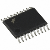
74ABT244CMTC Fairchild Semiconductor, 74ABT244CMTC Datasheet - Page 4

74ABT244CMTC
Manufacturer Part Number
74ABT244CMTC
Description
IC BUFF/DVR TRI-ST DUAL 20TSSOP
Manufacturer
Fairchild Semiconductor
Series
74ABTr
Specifications of 74ABT244CMTC
Logic Type
Buffer/Line Driver, Non-Inverting
Number Of Elements
2
Number Of Bits Per Element
4
Current - Output High, Low
32mA, 64mA
Voltage - Supply
4.5 V ~ 5.5 V
Operating Temperature
-40°C ~ 85°C
Mounting Type
Surface Mount
Package / Case
20-TSSOP
Logic Family
ABT
Number Of Channels Per Chip
8
Polarity
Non-Inverting
Supply Voltage (max)
5.5 V
Supply Voltage (min)
4.5 V
Maximum Operating Temperature
+ 85 C
Mounting Style
SMD/SMT
High Level Output Current
- 32 mA
Low Level Output Current
64 mA
Minimum Operating Temperature
- 40 C
Number Of Lines (input / Output)
8 / 3
Output Type
3-State
Propagation Delay Time
3.6 ns at 5 V
Lead Free Status / RoHS Status
Lead free / RoHS Compliant
Available stocks
Company
Part Number
Manufacturer
Quantity
Price
Part Number:
74ABT244CMTCX
Manufacturer:
FAIRCHILD/仙童
Quantity:
20 000
www.fairchildsemi.com
t
(Note 12)
t
(Note 12)
t
(Note 16)
t
(Note 12)
t
(Note 13)
C
C
OSHL
OSLH
PS
OST
PV
Skew
Note 12: Skew is defined as the absolute value of the difference between the actual propagation delays for any two separate outputs of the same device.
The specification applies to any outputs switching HIGH-to-LOW (t
HIGH-to-LOW (t
Note 13: Propagation delay variation for a given set of conditions (i.e., temperature and V
tested.
Note 14: This specification is guaranteed but not tested. The limits apply to propagation delays for all paths described switching in phase
(i.e., all LOW-to-HIGH, HIGH-to-LOW, etc.)
Note 15: These specifications guaranteed but not tested. The limits represent propagation delays with 250 pF load capacitors in place of the 50 pF load
capacitors in the standard AC load.
Note 16: This describes the difference between the delay of the LOW-to-HIGH and the HIGH-to-LOW transition on the same pin. It is measured across all
the outputs (drivers) on the same chip, the worst (largest delta) number is the guaranteed specification. This specification is guaranteed but not tested.
Capacitance
Note 17: C
IN
OUT
Symbol
(Note 17)
Symbol
OUT
is measured at frequency f
OST
). The specification is guaranteed but not tested.
Input Capacitance
Output Capacitance
Pin to Pin Skew
HL Transitions
Pin to Pin Skew
LH Transitions
Duty Cycle
LH–HL Skew
Pin to Pin Skew
LH/HL Transitions
Device to Device Skew
LH/HL Transitions
Parameter
Parameter
1 MHz, per MIL-STD-883, Method 3012.
OSHL
), LOW-to-HIGH (t
8 Outputs Switching
T
A
4
Typ
5.0
9.0
V
CC
C
(Note 14)
40 C to 85 C
L
Max
4.5V–5.5V
0.8
0.8
1.0
1.0
1.5
50 pF
OSLH
CC
) from device to device. This specification is guaranteed but not
), or any combination switching LOW-to-HIGH and/or
Units
pF
pF
8 Outputs Switching
T
A
V
V
V
CC
CC
CC
C
(Note 15)
L
40 C to 85 C
Max
4.5V–5.5V
1.8
1.8
2.5
2.5
3.0
0V
5.0V
250 pF
Conditions
T
A
25 C
Units
ns
ns
ns
ns
ns


