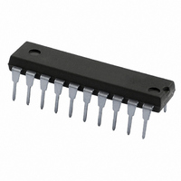
74ABT640N,602 NXP Semiconductors, 74ABT640N,602 Datasheet - Page 4

74ABT640N,602
Manufacturer Part Number
74ABT640N,602
Description
IC TRANSCEIVER 3ST 8BIT 20DIP
Manufacturer
NXP Semiconductors
Series
74ABTr
Datasheet
1.74ABT640N602.pdf
(10 pages)
Specifications of 74ABT640N,602
Logic Type
Transceiver, Inverting
Package / Case
20-DIP (0.300", 7.62mm)
Number Of Elements
1
Number Of Bits Per Element
8
Current - Output High, Low
32mA, 64mA
Voltage - Supply
4.5 V ~ 5.5 V
Operating Temperature
-40°C ~ 85°C
Mounting Type
Through Hole
Logic Family
74ABT
Number Of Channels Per Chip
8
Input Level
TTL
Output Level
TTL
Output Type
3-State
High Level Output Current
- 32 mA
Low Level Output Current
64 mA
Propagation Delay Time
3.1 ns
Supply Voltage (max)
5.5 V
Supply Voltage (min)
4.5 V
Maximum Operating Temperature
+ 85 C
Function
Bidirectional Transceiver
Input Bias Current (max)
30000 uA
Minimum Operating Temperature
- 40 C
Mounting Style
Through Hole
Polarity
Inverting
Number Of Circuits
8
Lead Free Status / RoHS Status
Lead free / RoHS Compliant
Lead Free Status / RoHS Status
Lead free / RoHS Compliant, Lead free / RoHS Compliant
Other names
74ABT640N
74ABT640N
935056030602
74ABT640N
935056030602
1. Not more than one output should be tested at a time, and the duration of the test should not exceed one second.
2. This is the increase in supply current for each input at 3.4V.
3. This parameter is valid for any V
Philips Semiconductors
RECOMMENDED OPERATING CONDITIONS
DC ELECTRICAL CHARACTERISTICS
NOTES:
1998 Jan 16
SYMBOL
I
I
SYMBOL
IH
IL
Octal transceiver with direction pin, inverting
(3-State)
I
transition time of up to 100 sec is permitted.
PU
I
V
I
I
I
I
T
V
V
V
OFF
+ I
+ I
CEX
CCH
CCL
CCZ
V
I
V
I
I
amb
I
OH
t/ v
OH
V
OL
OL
I
/I
O
CC
CC
IK
I
IH
IL
I
PD
OZH
OZL
Input clamp voltage
High-level output voltage
Low-level output voltage
Input leakage
current
Power-off leakage current
Power-up/down 3-State
output current
3-State output High current
3-State output Low current
Output High leakage current
Output current
Quiescent supply current
Additional supply current per
input pin
DC supply voltage
Input voltage
High-level input voltage
Low-level input voltage
High-level output current
Low-level output current
Input transition rise or fall rate
Operating free-air temperature range
PARAMETER
2
3
1
Control pins
Data pins
CC
between 0V and 2.1V, with a transition time of up to 10msec. From V
V
V
V
V
V
V
V
V
V
V
V
V
V
V
V
V
V
V
other inputs at V
V
PARAMETER
CC
CC
CC
CC
CC
CC
CC
CC
CC
CC
CC
CC
CC
CC
CC
CC
I
CC
OE
= GND or V
= 4.5V; I
= 4.5V; I
= 5.0V; I
= 4.5V; I
= 4.5V; I
= 5.5V; V
= 5.5V; V
= 0.0V; V
= 2.1V; V
= 5.5V; V
= 5.5V; V
= 5.5V; V
= 5.5V; V
= 5.5V; Outputs High, V
= 5.5V; Outputs Low, V
= 5.5V; Outputs 3-State;
= 5.5V; one input at 3.4V,
= Don’t care
TEST CONDITIONS
IK
OH
OH
OH
OL
I
I
I
O
O
O
O
O
CC
= GND or 5.5V
= GND or 5.5V
or V
= –18mA
= 0.5V; V
= 2.7V; V
= 0.5V; V
= 5.5V; V
= 2.5V
= 64mA; V
= –3mA; V
= –3mA; V
= –32mA; V
CC
O
or GND
4.5V
I
I
I
I
4
= GND or V
= V
= V
= GND or V
I
I
I
I
= V
= V
= V
I
I
= GND or V
= V
= GND or V
IL
IL
IL
IL
IL
or V
or V
IL
or V
or V
or V
or V
IH
IH
IH
IH
IH
CC
CC
IH
CC
;
CC
Min
–50
2.5
3.0
2.0
T
amb
Min
–40
4.5
2.0
0
0
–100
–0.9
0.42
–5.0
0.05
Typ
2.9
3.4
2.4
0.01
5.0
5.0
= +25 C
50
24
50
5.0
5.0
5
CC
LIMITS
LIMITS
–180
= 2.1V to V
Max
–1.2
0.55
–50
250
250
1.5
100
100
50
50
30
1.0
50
Max
V
–32
+85
5.5
0.8
T
64
5
Min
–50
CC
amb
2.5
3.0
2.0
74ABT640
to +85 C
CC
Product specification
= –40 C
= 5V 10% a
–180
Max
–1.2
0.55
–50
250
250
1.5
100
100
50
50
30
1.0
50
UNIT
ns/V
mA
mA
V
V
V
V
C
UNIT
mA
mA
mA
V
V
V
V
V
A
A
A
A
A
A
A
A
A


