IRF840 Advanced Power Electronics Corp., IRF840 Datasheet - Page 2
IRF840
Manufacturer Part Number
IRF840
Description
APEC MOSFET provide the power designer with the best combination of fast switching , lower on-resistance and reasonable cost
Manufacturer
Advanced Power Electronics Corp.
Datasheet
1.IRF840.pdf
(4 pages)
Specifications of IRF840
Vds
500V
Vgs
±20V
Rds(on) / Max(m?) Vgs@10v
850
Qg (nc)
45
Qgs (nc)
7
Qgd (nc)
25
Id(a)
8
Pd(w)
125
Configuration
Single N
Package
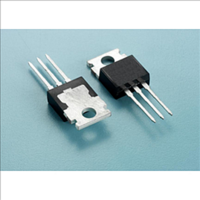
TO-220
Available stocks
Company
Part Number
Manufacturer
Quantity
Price

Part Number:
IRF840
Manufacturer:
IR
Quantity:
20 000
Part Number:
IRF840(HJ)
Manufacturer:
华晶
Quantity:
20 000
Company:
Part Number:
IRF840(SAM)
Manufacturer:
SAMSUNG
Quantity:
581
Company:
Part Number:
IRF840A
Manufacturer:
IR
Quantity:
12 500
Company:
Part Number:
IRF840AL
Manufacturer:
IR
Quantity:
12 500
Part Number:
IRF840APBF
Manufacturer:
VISHAY/威世
Quantity:
20 000


THIS PRODUCT IS ELECTROSTATIC SENSITIVE, PLEASE HANDLE WITH CAUTION.
THIS PRODUCT HAS BEEN QUALIFIED FOR USE IN CONSUMER APPLICATIONS. APPLICATIONS OR USE IN LIFE SUPPORT
OR OTHER SIMILAR MISSION-CRITICAL DEVICES OR SYSTEMS ARE NOT AUTHORIZED.
BV
R
V
g
I
I
Q
Q
Q
t
t
t
t
C
C
C
R
V
t
Q
Notes:
1.Pulse width limited by Max. junction temperature.
2.Starting T
3.Pulse test
IRF840
Electrical Characteristics@T
Source-Drain Diode
DSS
GSS
d(on)
r
d(off)
f
rr
fs
GS(th)
SD
DS(ON)
iss
oss
rss
g
g
gs
gd
rr
DSS
Symbol
Symbol
j
=25
Drain-Source Breakdown Voltage
Static Drain-Source On-Resistance
Gate Threshold Voltage
Forward Transconductance
Drain-Source Leakage Current (T
Drain-Source Leakage Current (T
Gate-Source Leakage
Total Gate Charge
Gate-Source Charge
Gate-Drain ("Miller") Charge
Turn-on Delay Time
Rise Time
Turn-off Delay Time
Fall Time
Input Capacitance
Output Capacitance
Reverse Transfer Capacitance
Gate Resistance
Forward On Voltage
Reverse Recovery Time
Reverse Recovery Charge
o
C , V
DD
=50V , L=10mH , R
Parameter
Parameter
3
3
3
3
j
j
j
=25
=125
=25
G
=25Ω
o
C)
o
C)
o
C(unless otherwise specified)
V
V
V
V
V
V
V
I
V
V
V
I
R
R
V
V
f=1.0MHz
f=1.0MHz
T
I
dI/dt=100A/µs
D
D
S
j
GS
GS
DS
DS
DS
DS
GS
DS
GS
DD
GS
DS
G
D
=8A
=8A
=25℃, I
=8A,
=31Ω
=9.1Ω,V
=0V, I
=10V, I
=V
=10V, I
=500V, V
=400V
=±20V
=400V
=10V
=250V
=0V
=25V
GS
V
Test Conditions
Test Conditions
, I
GS
D
S
,
D
=8A, V
=1mA
D
D
V
=0
GS
=250uA
=4.8A
=4.8A
GS
GS
=10V
V
=0V
=0V
,
GS
=0V
Min.
Min.
500
2
-
-
-
-
-
-
-
-
-
-
-
-
-
-
-
-
-
-
-
1250 2000
Typ.
Typ.
270
515
4.2
1.6
8.6
45
25
12
31
48
33
85
7
-
-
-
-
-
-
-
±100
Max. Units
Max. Units
0.85
250
2.4
72
1.5
25
4
-
-
-
-
-
-
-
-
-
-
-
-
uA
uA
nA
nC
nC
nC
uC
pF
pF
pF
Ω
ns
ns
ns
ns
ns
V
V
S
Ω
V
2/4
Related parts for IRF840
Image
Part Number
Description
Manufacturer
Datasheet
Request
R
