AP3987I Advanced Power Electronics Corp., AP3987I Datasheet - Page 2
AP3987I
Manufacturer Part Number
AP3987I
Description
AP3987 series are specially designed as main switching devices for universal 90~265VAC off-line AC/DC converter applications
Manufacturer
Advanced Power Electronics Corp.
Datasheet
1.AP3987I.pdf
(5 pages)
Specifications of AP3987I
Vds
600V
Vgs
±30V
Rds(on) / Max(m?) Vgs@10v
1000
Qg (nc)
55
Qgs (nc)
9
Qgd (nc)
16
Id(a)
7
Pd(w)
37
Configuration
Single N
Package
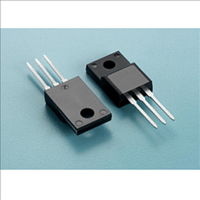
TO-220CFM


THIS PRODUCT IS SENSITIVE TO ELECTROSTATIC DISCHARGE, PLEASE HANDLE WITH CAUTION.
USE OF THIS PRODUCT AS A CRITICAL COMPONENT IN LIFE SUPPORT OR OTHER SIMILAR SYSTEMS IS NOT AUTHORIZED.
APEC DOES NOT ASSUME ANY LIABILITY ARISING OUT OF THE APPLICATION OR USE OF ANY PRODUCT OR CIRCUIT DESCRIBED
HEREIN; NEITHER DOES IT CONVEY ANY LICENSE UNDER ITS PATENT RIGHTS, NOR THE RIGHTS OF OTHERS.
APEC RESERVES THE RIGHT TO MAKE CHANGES WITHOUT FURTHER NOTICE TO ANY PRODUCTS HEREIN TO IMPROVE
RELIABILITY, FUNCTION OR DESIGN.
BV
R
V
g
I
I
Q
Q
Q
t
t
t
t
C
C
C
V
trr
Qrr
Notes:
1.Pulse width limited by max. junction temperature.
2.Starting T
3.Pulse test
Electrical Characteristics@T
Source-Drain Diode
AP3987I
DSS
GSS
d(on)
r
d(off)
f
fs
GS(th)
SD
DS(ON)
iss
oss
rss
g
gs
gd
DSS
Symbol
Symbol
j
=25
o
Drain-Source Breakdown Voltage
Static Drain-Source On-Resistance
Gate Threshold Voltage
Forward Transconductance
Drain-Source Leakage Current
Gate-Source Leakage
Total Gate Charge
Gate-Source Charge
Gate-Drain ("Miller") Charge
Turn-on Delay Time
Rise Time
Turn-off Delay Time
Fall Time
Input Capacitance
Output Capacitance
Reverse Transfer Capacitance
Forward On Voltage
Reverse Recovery Time
Reverse Recovery Charge
C , V
DD
=50V , L=1mH , R
Parameter
Parameter
3
3
3
3
G
j
=25
=25Ω
o
C(unless otherwise specified)
V
V
V
V
V
V
I
V
V
V
I
R
R
V
V
f=1.0MHz
I
I
dI/dt=100A/µs
D
D
S
S
GS
GS
DS
DS
DS
GS
DS
GS
DD
GS
DS
=7A
=7A
G
D
=7A, V
=7A, V
=43Ω
=10Ω,V
=V
=10V, I
=480V, V
=480V
=25V
=0V, I
=10V, I
=±30V
=10V
=300V
=0V
GS
Test Conditions
Test Conditions
GS
GS
, I
D
D
=0V
=0V,
=1mA
D
D
GS
=250uA
=5A
=5A
GS
=10V
=0V
Min.
Min.
600
2
-
-
-
-
-
-
-
-
-
-
-
-
-
-
-
-
-
2750 4400
Typ.
Typ.
100
160
530
8.6
55
16
15
15
32
5
9
6
-
-
-
-
-
-
±100
Max. Units
Max. Units
100
1.5
90
1
4
-
-
-
-
-
-
-
-
-
-
-
-
µC
uA
nA
nC
nC
nC
pF
pF
pF
Ω
ns
ns
ns
ns
ns
V
V
S
V
2/4
Related parts for AP3987I
Image
Part Number
Description
Manufacturer
Datasheet
Request
R
