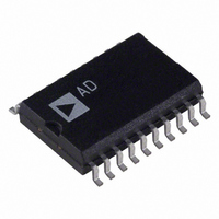
AD8321AR-REEL Analog Devices Inc, AD8321AR-REEL Datasheet

AD8321AR-REEL
Specifications of AD8321AR-REEL
Available stocks
Related parts for AD8321AR-REEL
AD8321AR-REEL Summary of contents
Page 1
FEATURES Linear in dB Gain Response Over >53 dB Range Drives Low Distortion >11 dBm Signal into 75 � Load: –53 dBc SFDR at 42 MHz Very Low Output Noise Level Maintains Constant 75 � Output Impedance Power-Up and ...
Page 2
AD8321–SPECIFICATIONS Parameter INPUT CHARACTERISTICS Specified AC Voltage Noise Figure Input Resistance Input Capacitance GAIN CONTROL INTERFACE Gain Range Maximum Gain Minimum Gain Gain Scaling Factor OUTPUT CHARACTERISTICS Bandwidth (–3 dB) Bandwidth Roll-Off Bandwidth Peaking Output Offset Voltage Output Noise Spectral ...
Page 3
LOGIC INPUTS (TTL/CMOS Logic) Parameter Logic “1” Voltage Logic “0” Voltage = 5 V) CLK, SDATA, DATEN Logic “1” Current (V INH = 0 V) CLK, SDATA, DATEN Logic “0” Current (V INL = Logic “1” Current ...
Page 4
... Exposure to absolute maximum rating conditions for extended periods may affect device reliability. Model Temperature Range AD8321AR –40∞C to +85∞C AD8321AR-REEL –40∞C to +85∞C 2 AD8321ARZ –40∞C to +85∞C 2 AD8321ARZ-REEL – ...
Page 5
GAIN CONTROL – Decimal Figure 4. Gain Error vs. Gain Control ...
Page 6
AD8321 34 MAX GAIN P = 11dBm OUT 10pF 0pF 20pF 50pF 100 FREQUENCY – MHz Figure 13. AC Response for ...
Page 7
OPERATIONAL DESCRIPTION The AD8321 is a digitally controlled variable gain power ampli fier that is optimized for driving cable multifunc tional bipolar device on a single silicon die, it incorporates all the analog features necessary ...
Page 8
AD8321 The attenuation setting in the AD8321 is determined by the 8-bit word in the data latch. The SDATA load sequence is initiated by a falling edge on DATEN. The gain control data (SDATA) is serially loaded (MSB first) into ...
Page 9
Basic Connection Figure 25 shows the basic schematic for operating the AD8321 in single-ended inverting mode. To operate in inverting mode, connect the input signal through an ac coupling capacitor to VIN–; VIN+ should be decoupled to ground with a ...
Page 10
AD8321 Varying the Gain and SPI Programming The gain of the AD8321 can be varied over a range from approximately – +26 dB, in increments of approximately 0.7526 dB per LSB. Programming the gain of ...
Page 11
Distortion and DOCSIS Care must be taken when selecting attenuation levels specified in Table I as the output signal from the AD8321 must compen sate for the losses resulting from any added attenuation as well as the insertion losses associated ...
Page 12
AD8321 Differential Input Option 2: Install the Mini-Circuits T1-6T KK81 1:1 transformer in the T1 location of the evaluation board. Jumpers J1, J2 and J3 should be applied pointing in the direction of the transformer. Apply an open circuit in ...
Page 13
TP1 C1 0.1�F J3 VIN– R1 82.5� TP4 VCC TP6 SDATA P1–5 TP7 R6 CLK P1–6 TP8 DATEN P1–2 TP9 PD P1– C14 C15 10�F 0.1�F TP5 GND V CC C10 C6 0.1�F 10�F R8 1k� V1 P1–8 ...
Page 14
AD8321 EVALUATION BOARD FEATURES AND OPERATION Figure 29. Evaluation Board Software Installation Figure 30. Evaluation Board Control Software –14– REV. A ...
Page 15
Figure 31. Screen Display of Windows-Based Control Software REV. A –15– AD8321 ...
Page 16
AD8321 Figure 32. Evaluation Board Silkscreen (Component Side) –16– REV. A ...
Page 17
Figure 33. Evaluation Board Layout (Component Side) REV. A Figure 34. Evaluation Board Layout (Solder Side) –17– AD8321 ...
Page 18
... ADS# 12-18-64 ADS# 12-18-32 ADS# 12-18-60 ADS# 12-18-43 ADS# 12-18-44 ADS# 11-2-38 ADS# 11-2-37 Comp. Mktg. Services ADS# 12-3-50 ADS# 12-7-7 ADS# AD8321AR E.M.C. ADS# 30-1-1 ADS# 30-16-3 ADS# 30-1-17 ADS# 30-6-6 ADS# 30-5-2 ADS# 30-7-6 –18– Ref Desc. C6 & C14 C1– ...
Page 19
Revision History Location 6/05—Data Sheet Changed from REV REV. A. Changes to ORDERING GUIDE ....................................................................................................................................................4 Updated OUTLINE DIMENSIONS.............................................................................................................................................19 REV. A OUTLINE DIMENSIONS 20-Lead Standard Small Outline Package [SOIC_W] Wide Body (R-20) Dimensions shown in millimeters and (inches) –19– ...
Page 20
–20– ...


