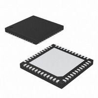
MAX9406ETM+T Maxim Integrated Products, MAX9406ETM+T Datasheet - Page 2

MAX9406ETM+T
Manufacturer Part Number
MAX9406ETM+T
Description
IC DVI/HDMI LVL SHIFTR 48TQFN-EP
Manufacturer
Maxim Integrated Products
Type
Level Shifterr
Datasheet
1.MAX9406ETJT.pdf
(11 pages)
Specifications of MAX9406ETM+T
Applications
Base Stations
Mounting Type
Surface Mount
Package / Case
48-TQFN Exposed Pad
Lead Free Status / RoHS Status
Lead free / RoHS Compliant
DisplayPort to DVI™/HDMI Level Shifter
ABSOLUTE MAXIMUM RATINGS
V
All Pins to GND...........................................-0.3V to (V
Short-Circuit Duration (all outputs).............................Continuous
Continuous Power Dissipation (T
Junction-to-Case Thermal Resistance (θ
Junction-to-Ambient Thermal Resistance (θ
DC ELECTRICAL CHARACTERISTICS
(V
Note 1: Package thermal resistances were obtained using the method described in JEDEC specification JESD51-7, using a 4-layer board.
For detailed information on package thermal considerations, refer to Application Note 4083 at www.maxim-ic.com/thermal-tutorial.
Stresses beyond those listed under “Absolute Maximum Ratings” may cause permanent damage to the device. These are stress ratings only, and functional
operation of the device at these or any other conditions beyond those indicated in the operational sections of the specifications is not implied. Exposure to
absolute maximum rating conditions for extended periods may affect device reliability.
2
OE INPUT
Input High Level
Input Low Level
Input Current
DDC_EN INPUT
Input High Level
Input Low Level
Input Current
HPD INPUT AND OUTPUT
Input High Level
Input Low Level
Input Current
HPD_SNK Pulldown Resistance
Output High Level
Output Low Level
DIFFERENTIAL INPUTS (IN_)
Differential Input High Threshold
Differential Input Low Threshold
Common Input Voltage
Common-Mode AC Tolerance
Differential Input Termination
CC
CC
32-Pin Thin QFN (derate 21.3mW/°C above +70°C) .1702mW
48-Pin Thin QFN (derate 27.8mW/°C above +70°C) .2222mW
32-Pin Thin QFN........................................................+1.7°C/W
48-Pin Thin QFN........................................................+0.8°C/W
32-Pin Thin QFN.........................................................+29°C/W
48-Pin Thin QFN.........................................................+25°C/W
_______________________________________________________________________________________
to GND ..............................................................-0.3V to +4V
= 3V to 3.6V, T
PARAMETER
A
= -40°C to +85°C, unless otherwise noted. Typical values are at V
A
= +70°C)
V
V
V
SYMBOL
C M _A C _P - P
I
OH-HPDB
OL-HPDB
IN-DDC
V
I
R
V
JC
V
IN-EN
V
V
V
V
V
V
I
R
COM
HPD
IN2
IDH
IH1
IH1
IH2
IDL
IL1
IL1
IL2
IN
) (Note 1)
JA
) (Note 1)
V
V
V
V
V
V
V
IN
IN
IN
ID
ID
COD
CM_AC_P-P
CC
= 0 to V
= 0 to V
= 0 to V
= V
= V
+ 0.3V)
= DC Avg [(V
IN+
IN+
- V
- V
CC
CC
CC
= (V
IN-
IN-
CONDITIONS
IN+
IN+
Operating Temperature Range ..…………………-40°C to +85°C
Junction Temperature ………………………………………+150°C
Storage Temperature Range ……………………-65°C to +150°C
ESD Protection
Lead Temperature (soldering, 10s).………………………+300°C
+ V
Human Body Model (R
IN_D_ and OUT_D_ to GND..........................................±1.5kV
+ V
IN-
) / 2 - V
IN-
) / 2]
COD
CC
= 3.3V, T
D
= 1.5kΩ, C
MIN
2.4
2.4
2.4
2.5
-50
40
40
0
0
A
= +25°C.)
TYP
0.18
1.43
100
S
24
80
60
= 100pF)
MAX
V
100
0.5
0.5
5.3
0.8
0.4
50
60
CC
2
UNITS
mV
mV
mV
kΩ
µA
µA
µA
Ω
V
V
V
V
V
V
V
V
V


