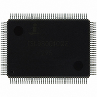
ISL98001CQZ-275 Intersil, ISL98001CQZ-275 Datasheet - Page 20

ISL98001CQZ-275
Manufacturer Part Number
ISL98001CQZ-275
Description
IC TRPL VIDEO DIGITIZER 128-MQFP
Manufacturer
Intersil
Type
Video Digitizerr
Datasheet
1.ISL98001IQZ-140.pdf
(31 pages)
Specifications of ISL98001CQZ-275
Applications
Digital TV, Displays, Digital KVM, Graphics Processing
Mounting Type
Surface Mount
Package / Case
128-MQFP, 128-PQFP
Lead Free Status / RoHS Status
Lead free / RoHS Compliant
Available stocks
Company
Part Number
Manufacturer
Quantity
Price
Company:
Part Number:
ISL98001CQZ-275
Manufacturer:
INTERSIL
Quantity:
772
Part Number:
ISL98001CQZ-275
Manufacturer:
INTERSIL
Quantity:
20 000
The ISL98001 can optionally decimate the incoming data to
provide a 4:2:2 output stream (configuration register
0x18[4] = 1) as shown in Table 2.
There is also a “compatibility mode”, enabled by setting bit 3
of register 0x18 to a 1, that outputs the U and V data with the
format used by the previous generation (“X980xx”) series of
AFEs, shown in Table 3.
Input Coupling
Inputs can be either AC-coupled (default) or DC-coupled (See
register 0x05[1]). AC coupling is usually preferred since it
allows video signals with substantial DC offsets to be accurately
digitized. The ISL98001 provides a complete internal
DC-restore function, including the DC restore clamp (See
Figure 7) and programmable clamp timing (registers 0x14,
0x15, 0x16, and 0x23).
When AC-coupled, the DC restore clamp is applied every line,
a programmable number of pixels after the trailing edge of
HSYNC. If register 0x05[5] = 0 (the default), the clamp will not
R(GB)
R(GB)
SIGNAL
SIGNAL
INPUT
INPUT
R(GB)
R(GB)
Pb
Pb
Pr
Pr
Y
Y
GND
GND
IN
IN
1
1
2
2
TABLE 2. YUV MAPPING (4:2:2)
TABLE 3. YUV MAPPING (4:2:2)
CHANNEL
CHANNEL
ISL98001
ISL98001
DC Restore
Clamp DAC
INPUT
INPUT
VGA1
VGA2
Green
Green
Blue
Blue
Red
Red
V
V
IN
IN
DC Restoration
+
-
V
CLAMP
20
ASSIGNMENT
ASSIGNMENT
ISL98001
ISL98001
OUTPUT
OUTPUT
Green
Green
Blue
Blue
Red
Red
PGA
GENERATION
CLAMP
FIGURE 7. VIDEO FLOW (INCLUDING ABLC)
U
U
Y
Y
driven low
driven low
OUTPUT
OUTPUT
SIGNAL
SIGNAL
0
0
0
0
Bandwidth
Y
V
Y
V
Input
Bandwidth
Control
1
0
1
1
Y
U
Y
U
2
2
2
2
ABLC
Block
Y
Y
V
V
To
3
3
2
3
ISL98001
be applied while the DPLL is coasting, preventing any clamp
voltage errors from composite sync edges, equalization pulses,
or Macrovision signals.
After the trailing edge of HSYNC, the DC restore clamp is
turned on after the number of pixels specified in the DC Restore
and ABLC Starting Pixel registers (0x14 and 0x15) has been
reached. The clamp is applied for the number of pixels
specified by the DC Restore Clamp Width Register (0x16). The
clamp can be applied to the back porch of the video, or to the
front porch (by increasing the DC Restore and ABLC Starting
Pixel registers so all the active video pixels are skipped).
If DC-coupled operation is desired, the input to the ADC will be
the difference between the input signal (R
that channel’s ground reference (RGB
SOG
For component YPbPr signals, the sync signal is embedded
on the Y channel’s video, which is connected to the green
input, hence the name SOG (Sync on Green). The horizontal
sync information is encoded onto the video input by adding
the sync tip during the blanking interval. The sync tip level is
typically 0.3V below the video black level.
To minimize the loading on the Green channel, the SOG input
for each of the green channels should be AC-coupled to the
ISL98001 through a series combination of a 10nF capacitor
and a 500Ω resistor. Inside the ISL98001, a window
comparator compares the SOG signal with an internal 4-bit
programmable threshold level reference ranging from 0mV to
300mV below the minimum sync level. The SOG threshold
level, hysteresis, and low-pass filter is programmed via
register 0x04. If the Sync-On-Green function is not needed,
the SOG
SYNC Processing
The ISL98001 can process sync signals from 3 different
sources: discrete HSYNC and VSYNC, composite sync on
Offset
DAC
Compensation (ABLC™) Loop
10
IN
8 bit ADC
Automatic Black Level
pin(s) may be left unconnected.
ABLC™
Offset
Fixed
10
10
ABLC™
8
Registers
Control
Offset
ABLC™
GND
8
IN
8
1 in that example).
1, for example) and
Offset
Fixed
0x00
8
8
September 21, 2010
To Output
Formatter
FN6148.5


