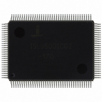
ISL98001CQZ-170 Intersil, ISL98001CQZ-170 Datasheet - Page 26

ISL98001CQZ-170
Manufacturer Part Number
ISL98001CQZ-170
Description
IC TRPL VIDEO DIGITIZER 128-MQFP
Manufacturer
Intersil
Type
Video Digitizerr
Datasheet
1.ISL98001IQZ-140.pdf
(31 pages)
Specifications of ISL98001CQZ-170
Applications
Digital TV, Displays, Digital KVM, Graphics Processing
Mounting Type
Surface Mount
Package / Case
128-MQFP, 128-PQFP
Lead Free Status / RoHS Status
Lead free / RoHS Compliant
Available stocks
Company
Part Number
Manufacturer
Quantity
Price
Company:
Part Number:
ISL98001CQZ-170
Manufacturer:
INTES
Quantity:
274
Part Number:
ISL98001CQZ-170
Manufacturer:
INTERSIL
Quantity:
20 000
Crystal Oscillator
An external 22MHz to 27MHz crystal supplies the low-jitter
reference clock to the DPLL. The absolute frequency of this
crystal within this range is unimportant, as is the crystal’s
temperature coefficient, allowing use of less expensive,
lower-grade crystals.
As an alternative to a crystal, the XTAL
with a 3.3V CMOS-level external clock source at any
frequency between 22MHz and 33.5MHz. The ISL98001’s
jitter specification assumes a low-jitter crystal source. If the
external clock source has increased jitter, the sample clock
generated by the DPLL may exhibit increased jitter as well.
Reset
The ISL98001 has a Power On Reset (POR) function that
resets the chip to its default state when power is initially
applied, including resetting all the registers to their default
settings as described in the Register Listing. The external
RESET pin duplicates the reset function of the POR without
having to cycle the power supplies. The RESET pin does not
need to be used in normal operation and can be tied high.
Initialization
The ISL98001 initializes with default register settings for an
AC-coupled, 640x480 RGB input on the VGA1 channel, with
a 24-bit output. An input signal meeting these conditions will
be output on the databus without writing to any of the
configuration registers. The configuration registers will need
to be changed as required to support other resolutions,
different input channels, different sync sources, phase
optimization etc.
The ISL98001-275 requires one additional register write to
operate at their maximum speed. The ISL98001 generates
an internal reference clock equal to the crystal frequency
times the value in register 0x2B (nominally 0x14 or
20 decimal). The typical value of this clock is therefore
500MHz (25MHz*20). The minimum value of this clock is
360MHz.
This internal clock needs to be greater than 2 times the PLL
pixel rate. The nominal value of 500MHz therefore supports
pixel rates up to 250MHz. To achieve pixel rates of 275MHz,
or to work with lower frequency crystals, the multiplier in
register 0x2B must be programmed using Equation 2:
For example, if the maximum pixel clock is 263MHz (QXGA),
and the crystal frequency is 24MHz, then register 0x2B
should be set to 1 + INT(2*263/24) = 1 + INT(21.917) =
1 + 21 = 22 = 0x16. Table 9 illustrates the compensation
values required to operate the ISL98001-275 at its maximum
speed of 275MHz. If lower maximum Pixel Clock frequencies
are needed, using the formula above to reduce the value of
register 0x2B will reduce power consumption.
0x2B value
=
INT 2
⎛
⎜
⎝
f
---------------------------------------- -
MAX_PIXELCLK
f
CRYSTAL
26
⎞
⎟
⎠
+
1
IN
pin can be driven
(EQ. 2)
ISL98001
Reducing Power Dissipation
It is possible to reduce the total power consumption of the
ISL98001 in applications where power is a concern. There are
several techniques that can be used to reduce power
consumption:
• Internal Digital Voltage Regulator. The ISL98001 features
• Internal Analog Voltage Regulator. The ISL98001 also
• Buffering Digital Outputs. Switching 24 or 48 data output
• Internal Reference Frequency. The crystal frequency is
Standby Mode
The ISL98001 can be placed into a low power standby mode
by writing a 0x0F to register 0x1B, powering down the triple
ADCs, the DPLL, and most of the internal clocks.
CRYSTAL FREQUENCY RANGE
TABLE 9. CRYSTAL MULTIPLIER FOR 275MHz PIXEL RATE
a 3.3V to 1.9V voltage regulator (pins VREG
VREG
typically sources 100mA at 1.9V, dissipating up to 140mW in
heat. Providing an external, clean 1.8V supply to the V
V
dissipation. The external 1.8V supply should ramp up after
(or at the same time as) the digital 3.3V (V
features a 3.3V to 1.9V voltage regulator for the low voltage
analog supply. This voltage appears on the V
Unlike the digital low voltage supply, there are no “in” and
“out” connections for this regulator. However, this internal
regulator can only source voltage, and can be effectively
bypassed by driving the V
clean 2.0V supply. The external 2.0V supply should ramp up
after (or at the same time as) the analog 3.3V (V
pins into a capacitive bus can consume significant current.
The higher the capacitance on the external databus, the
higher the switching current. To minimize current
consumption inside the ISL98001, minimize bus capacitance
and/or insert data buffers such as the SN64AVC16827
between the ISL98001’s data outputs and the external
databus.
multiplied by the value in register 0x2B to generate an
internal high frequency reference clock. For pixel rates up to
160MHz, this internal frequency should be set to 400MHz
±10% for minimum power consumption. For example, for a
33MHz frequency at XTAL
a value of 0x0C to minimize power. For pixel rates greater
than 160MHz, the register 0x2B value should be set using
Equation 2 in the “Initialization” section on page 26.
PLL
, and V
OUT
25.0 to 26.2
) for the low voltage digital supply. This regulator
23 to 23.9
23.9 to 25
26.2 to 27
COREADC
(MHz)
will substantially reduce power
BYPASS
IN
, register 0x2B should be set to
pins with an external,
DECIMAL
REGISTER 0x2B
24
23
22
21
D
) supply.
VALUE
IN
BYPASS
September 21, 2010
and
A
) supply.
0x18
0x17
0x16
0x15
HEX
CORE
FN6148.5
pins.
,


