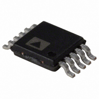
ADA4417-3ARMZ Analog Devices Inc, ADA4417-3ARMZ Datasheet

ADA4417-3ARMZ
Specifications of ADA4417-3ARMZ
Available stocks
Related parts for ADA4417-3ARMZ
ADA4417-3ARMZ Summary of contents
Page 1
... With 1 dB frequency flatness out to 38 MHz, and rejection at 75 MHz, the ADA4417-3 can handle the most demanding HD video applications. The ADA4417-3 operates on a single 3 supply well-suited for applications where power consumption is critical. A disable feature allows for further power conservation by reducing the supply current to 10 μ ...
Page 2
... ADA4417-3 TABLE OF CONTENTS Features .............................................................................................. 1 Applications ....................................................................................... 1 Functional Block Diagram .............................................................. 1 General Description ......................................................................... 1 Revision History ............................................................................... 2 Specifications ..................................................................................... 3 Absolute Maximum Ratings ............................................................ 5 Thermal Resistance ...................................................................... 5 ESD Caution .................................................................................. 5 Pin Configuration and Function Descriptions ............................. 6 Typical Performance Characteristics ............................................. 7 Test Circuit ...................................................................................... 11 REVISION HISTORY 11/09—Rev Rev. A Changes to Input and Output Coupling ...................................... 13 Changes to Figure 28 ...................................................................... 14 Updated Outline Dimensions ....................................................... 15 7/06— ...
Page 3
... V p MHz MHz, input referred 275 Ω MHz MHz to 36 MHz Modulated 10 step ramp, sync tip Modulated 10 step ramp, sync tip MHz, DISABLE = 0 DCO = 0 DCO = 1 DCO = 0, DISABLE = 0 DCO = 0 Rev Page ADA4417-3 Min Typ Max Unit 70 100 142 See Note 2 0.08 4. ...
Page 4
... ADA4417 3 25° 1 Table 2. Parameter OVERALL PERFORMANCE DC Offset Input Voltage Range Output Voltage Range Linear Output Current DC Voltage Gain Integrated Voltage Noise Filter Input Bias Current Slew Rate Settling Time to 0.5% Output Overdrive Recovery Total Harmonic Distortion Gain Matching FILTER DYNAMIC PERFORMANCE − ...
Page 5
... Package Type θ JA 10-Lead MSOP 130 Maximum Power Dissipation The maximum safe power dissipation in the ADA4417-3 package is limited by the associated rise in junction temperature ( the die. At approximately 150°C, which is the glass J transition temperature, the plastic changes its properties. Even temporarily exceeding this temperature limit can change the stresses that the package exerts on the die, permanently shifting the parametric performance of the ADA4417-3 ...
Page 6
... Pr/R OUT 7 GND 8 Pb/B OUT 9 VCC 10 Y/G OUT Y/G IN Y/G OUT 1 10 DISABLE VCC 2 9 ADA4417-3 Pb/B IN Pb/B OUT 3 8 TOP VIEW (Not to Scale) DCO GND 4 7 Pr/R IN Pr/R OUT 5 6 Figure 3. Pin Configuration Description Y/G HD Video Input Disable/Power Down (Active Low) ...
Page 7
... Rev Page ADA4417-3 = 150 Ω, DCO = 1, unless otherwise noted. L BLACK LINE 3.3V S GRAY LINE FREQUENCY (MHz) Figure 7. Flatness Response vs. Supply BLACK LINE 75Ω L GRAY LINE 150Ω ...
Page 8
... ADA4417 BLACK LINE 0.2V p GRAY LINE 2.0V p-p S –3 –6 –9 –12 –15 –18 –21 –24 –27 –30 –33 –36 –39 –42 –45 – FREQUENCY (MHz) Figure 10. Frequency Response vs. Amplitude 10 REFERRED TO INPUT 0 –10 –20 –30 –40 –50 –60 –70 –80 0.01 ...
Page 9
... V S 275 250 225 200 175 100ns/DIV 150 –40 Figure 21. Output Saturation Voltage vs. Temperature Rev Page ADA4417-3 2 × INPUT OUTPUT 1.0%, 61ns ERROR 0.5%, 63ns 50ns/DIV Figure 19. Settling Time DISABLE INPUT OUTPUT 1µs/DIV Figure 20. Enable Turn Off Time = 5V –25 – ...
Page 10
... ADA4417-3 30 BLACK LINE 3.3V S GRAY LINE DCO = DCO = –40 –30 –20 – TEMPERATURE (°C) Figure 22. Supply Current vs. Temperature 5.0 4.5 4.0 DCO = 1 3.5 3.0 DCO = 0 2.5 2.0 1.5 1.0 0.5 0 –0.25 0.25 0.75 1.25 INPUT VOLTAGE (V) Figure 23. Output Voltage vs. Input Voltage ...
Page 11
... TEST CIRCUIT NETWORK R = 150Ω ANALYZER 50Ω 118Ω T DUT 50Ω 86.6Ω MINIMUM-LOSS MATCHING NETWORK LOSS CALIBRATED OUT Figure 25. Basic Test Circuit for Swept Frequency Measurements Rev Page ADA4417-3 NETWORK ANALYZER Rx 50Ω ...
Page 12
... ADA4417-3 THEORY OF OPERATION The ADA4417 low cost, integrated video filtering and driving solution that offers a 38 MHz bandwidth to meet the requirements of high definition video. Each of the three filters has a sixth-order Butterworth response that includes group delay equalization. Group delay variation from 1 MHz to 36 MHz is only 5 ns, resulting in greater stop-band attenuation and minimal phase distortion ...
Page 13
... DVDs, and a like without the need for a separate output buffer. DISABLE The ADA4417-3 includes a disable feature that can be used to save power when a particular device is not in use. The disable feature is asserted by pulling the DISABLE pin to ground. ...
Page 14
... DAC outputs of a video encoder. Figure 28 illustrates how to use the ADA4417-3 in this type of application with an ADV7322 video encoder in a single-supply application with ac-coupled outputs. ADV7322 VIDEO ENCODER VIDEO DAC OUTPUTS Figure 28. The ADA4417-3 Applied as a Video Reconstruction Filter Following the ADV7322 5V (ANALOG) 0.1µF 9 VCC DC OFFSET 4 ...
Page 15
... OUTLINE DIMENSIONS IDENTIFIER ORDERING GUIDE Model Temperature Range ADA4417-3ARMZ 1 −40°C to +85°C 1 ADA4417-3ARMZ-R7 −40°C to +85°C ADA4417-3ARMZ-RL 1 −40°C to +85° RoHS Compliant part. 3.10 3.00 2.90 5. 3.10 4.90 3.00 4.65 1 2.90 5 PIN 1 0.50 BSC 0.95 15° MAX 0.85 1 ...
Page 16
... ADA4417-3 NOTES ©2006–2009 Analog Devices, Inc. All rights reserved. Trademarks and registered trademarks are the property of their respective owners. D06221-0-11/09(A) Rev Page ...


