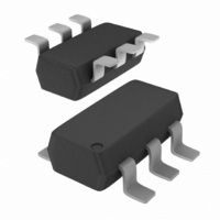
NCS2201SN1T1 ON Semiconductor, NCS2201SN1T1 Datasheet - Page 9

NCS2201SN1T1
Manufacturer Part Number
NCS2201SN1T1
Description
IC COMP 1V LP ENABLE 6-TSOP
Manufacturer
ON Semiconductor
Series
NCS2200r
Type
General Purposer
Datasheet
1.NCS2201SN1T1.pdf
(16 pages)
Specifications of NCS2201SN1T1
Number Of Elements
1
Output Type
Complementary, Rail-to-Rail
Voltage - Supply
0.85 V ~ 6 V
Mounting Type
Surface Mount
Package / Case
SC-74, SOT-457
Lead Free Status / RoHS Status
Contains lead / RoHS non-compliant
Other names
NCS2201SN1T1OSTR
Available stocks
Company
Part Number
Manufacturer
Quantity
Price
Part Number:
NCS2201SN1T1
Manufacturer:
ON/安森美
Quantity:
20 000
Part Number:
NCS2201SN1T1G
Manufacturer:
ON/安森美
Quantity:
20 000
OPERATING DESCRIPTION
power comparator family. This series is designed for
rail−to−rail input and output performance. These devices
consume only 10 mA of supply current while achieving a
typical propagation delay of 1.1 ms at a 20 mV input
overdrive. Figures 10 and 11 show propagation delay with
various input overdrives. This comparator family is
guaranteed to operate at a low voltage of 0.85 V up to 6.0 V.
This is accomplished by the use of a modified analog CMOS
process that implements depletion MOSFET devices. The
common−mode input voltage range extends 0.1 V beyond
the upper and lower rail without phase inversion or other
adverse effects. This series is available in the SOT23−5 and
SOT23−6 package. Additionally, the NCS2200 device is
available in the tiny QFN 2x2.2 package.
externally controlled. This feature allows significantly
lower current consumption of 0.3 mA. This makes the
devices suitable for implementation in power sensitive
applications such as portable electronics. The enable
function is active high when connected to the V
The NCS2200 Series is an industry first sub−one volt, low
The SOT23−6 features the enable function, which can be
IN (+)
IN (−)
Figure 17. NCS2200/1SNxT1 Complementary
Output Configuration
V
V
CC
EE
Output
CC
NCS2200 Series
http://onsemi.com
pin.
9
When the enable pin is driven low (device disabled), output
tri−state mode is activated. The device will remain in this
mode and will not respond to any changes at the inputs of the
comparator. In order to pull the device out of tri−state mode,
the enable upper voltage threshold must be met. Figure 15
shows the enable input voltage required to either enable or
disable the device, with a variance in supply voltage. In
addition, these devices have a typical internal hysteresis of
"8.0 mV. This allows for greater noise immunity and clean
output switching.
Output Stage
output stage that has capability of driving a rail−to−rail
output swing with a load ranging up to 5.0 mA. It is designed
such that shoot−through current is minimized while
switching. This feature eliminates the need for bypass
capacitors under most circumstances.
stage that can be pulled up to 6.0 V (max) with an external
resistor. This facilitates mixed voltage system applications.
The NCS2200/1 has a complementary P and N channel
The NCS2202/3 has an open drain N−channel output
IN (+)
IN (−)
Figure 18. NCS2202/3SNxT1 Open Drain
Output Configuration
V
V
CC
EE
Output


