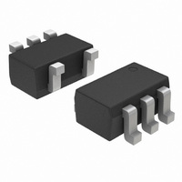
NCS2200SQ2T2G ON Semiconductor, NCS2200SQ2T2G Datasheet - Page 9

NCS2200SQ2T2G
Manufacturer Part Number
NCS2200SQ2T2G
Description
IC COMPARATOR LV LP OD SC70-5
Manufacturer
ON Semiconductor
Series
NCS2200r
Type
General Purposer
Datasheet
1.NCS2200AMUT1G.pdf
(17 pages)
Specifications of NCS2200SQ2T2G
Number Of Elements
1
Output Type
Complementary, Rail-to-Rail
Voltage - Supply
0.85 V ~ 6 V
Mounting Type
Surface Mount
Package / Case
6-TSSOP (5 lead), SC-88A, SOT-353
Number Of Elements
1
Technology
CMOS
Input Offset Voltage
5mV
Input Bias Current (typ)
10nA
Response Time
1.1us
Single Supply Voltage (typ)
3/5V
Dual Supply Voltage (typ)
Not RequiredV
Supply Current (max)
0.015mA
Power Supply Requirement
Single
Common Mode Rejection Ratio
70dB
Power Supply Rejection Ratio
80dB
Single Supply Voltage (min)
850mV
Single Supply Voltage (max)
6V
Dual Supply Voltage (min)
Not RequiredV
Dual Supply Voltage (max)
Not RequiredV
Operating Temp Range
-40C to 105C
Operating Temperature Classification
Industrial
Mounting
Surface Mount
Pin Count
5
Package Type
SC-70
Lead Free Status / RoHS Status
Lead free / RoHS Compliant
Other names
NCS2200SQ2T2G
NCS2200SQ2T2GOSTR
NCS2200SQ2T2GOSTR
Available stocks
Company
Part Number
Manufacturer
Quantity
Price
Company:
Part Number:
NCS2200SQ2T2G
Manufacturer:
ON
Quantity:
310 000
Part Number:
NCS2200SQ2T2G
Manufacturer:
ON/安森美
Quantity:
20 000
OPERATING DESCRIPTION
power comparator family. This series is designed for
rail−to−rail input and output performance. These devices
consume only 10 mA of supply current while achieving a
typical propagation delay of 1.1 ms at a 20 mV input
overdrive. Figures 10 and 11 show propagation delay with
various input overdrives. This comparator family is
guaranteed to operate at a low voltage of 0.85 V up to 6.0 V.
This is accomplished by the use of a modified analog CMOS
process that implements depletion MOSFET devices. The
common−mode input voltage range extends 0.1 V beyond
the upper and lower rail without phase inversion or other
adverse effects. This series is available in the SOT−23−5
The NCS2200 Series is an industry first sub−one volt, low
IN (+)
IN (−)
Complementary Output Configuration
Figure 15. NCS2200SNxT1/NCS2200A
V
V
CC
EE
The oscillation frequency can be programmed as follows:
C
x
Figure 17. Schmitt Trigger Oscillator
Output
IN (+)
IN (−)
http://onsemi.com
f + 1
NCS
2200
V
T
CC
+
9
2.2 R x C x
R
OUT
x
package. Additionally, the NCS2200 device is available in
the tiny DFN 2x2.2 package and the SC70−5 package.
NCS2200A is available in UDFN package.
Output Stage
output stage that has capability of driving a rail−to−rail
output swing with a load ranging up to 5.0 mA. It is designed
such that shoot−through current is minimized while
switching. This feature eliminates the need for bypass
capacitors under most circumstances.
that can be pulled up to 6.0 V (max) with an external resistor.
This facilitates mixed voltage system applications.
1
The NCS2200 has a complementary P and N Channel
The NCS2202 has an open drain N−channel output stage
IN (+)
IN (−)
Figure 16. NCS2202SNxT1 Open Drain
R
R
2
1
V
Output Configuration
O
V
V
CC
EE
Output


