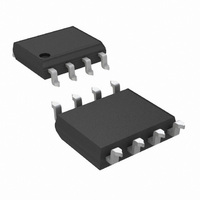
LMV762MAX/NOPB National Semiconductor, LMV762MAX/NOPB Datasheet - Page 8

LMV762MAX/NOPB
Manufacturer Part Number
LMV762MAX/NOPB
Description
IC COMP PREC W/P-POP LV 8-SOIC
Manufacturer
National Semiconductor
Type
General Purposer
Datasheet
1.LMV761MFNOPB.pdf
(12 pages)
Specifications of LMV762MAX/NOPB
Number Of Elements
2
Output Type
Push-Pull
Voltage - Supply
2.7 V ~ 5 V
Mounting Type
Surface Mount
Package / Case
8-SOIC (0.154", 3.90mm Width)
Lead Free Status / RoHS Status
Lead free / RoHS Compliant
Other names
LMV762MAX
Available stocks
Company
Part Number
Manufacturer
Quantity
Price
Part Number:
LMV762MAX/NOPB
Manufacturer:
TI/德州仪器
Quantity:
20 000
www.national.com
Application Information
BASIC COMPARATOR
A basic comparator circuit is used to convert analog input
signals to digital output signals. The comparator compares an
input voltage (V
voltage (V
output (V
V
HYSTERESIS
The basic comparator configuration may oscillate or produce
a noisy output if the applied differential input is near the
comparator's input offset voltage. This tends to occur when
the voltage on one input is equal or very close to the other
input voltage. Adding hysteresis can prevent this problem.
Hysteresis creates two switching thresholds (one for the rising
input voltage and the other for the falling input voltage). Hys-
teresis is the voltage difference between the two switching
thresholds. When both inputs are nearly equal, hysteresis
causes one input to effectively move quickly past the other.
Thus, moving the input out of the region in which oscillation
may occur.
Hysteresis can easily be added to a comparator in a non-in-
verting configuration with two resistors and positive feedback
Figure
up to V
The output will switch from high to low when V
where V
The Hysteresis is the difference between V
REF
= ((V
, the output voltage (V
2. The output will switch from low to high when V
IN1
IN2
REF
O
, where V
REF
) is low (V
is calculated by
(R
) at the inverting pin. If V
V
FIGURE 1. Basic Comparator
IN2
1
IN
+R
) at the non-inverting input to the reference
V
= (V
2
IN1
IN1
))/R
ΔV
REF
is calculated by
OL
= (V
2
= V
IN
)-((V
). However, if V
(R
O
REF
= V
CC
1
) is high (V
+R
REF
(R
IN1
R
2
(R
1
1
) – V
/R
+R
- V
1
2
+R
2
IN2
))/R
CC
IN
2
OH
)) - (V
is less than V
R
2
).
IN
20037028
1
)/R
IN1
is greater than
CC
2
IN
and V
R
falls to V
20037031
1
))/R
IN2
REF
IN
2
.
)
rises
the
IN2
,
8
INPUT
The LMV761/LMV762 have near zero input bias current. This
allows very high resistance circuits to be used without any
concern for matching input resistances. This also allows the
use of very small capacitors in R-C type timing circuits. This
reduces the cost of the capacitors and amount of board space
used.
SHUTDOWN MODE
The LMV761 features a low-power shutdown pin that is acti-
vated by driving SD low. In shutdown mode, the output is in
a high impedance state, supply current is reduced to 20nA
and the comparator is disabled. Driving SD high will turn the
comparator on. The SD pin should not be left unconnected
due to the fact that it is a high impedance input. When left
unconnected, the output will be at an unknown voltage. Also
do not three-state the SD pin.
The maximum input voltage for SD is 5.5V, referred to ground
and is not limited by V
drive SD while V
The logic threshold limits for SD are proportional to V
BOARD LAYOUT AND BYPASSING
The LMV761/LMV762 is designed to be stable and oscillation
free, but it is still important to include the proper bypass ca-
pacitors and ground pickups. Ceramic 0.1μF capacitors
should be placed at both supplies to provide clean switching.
Minimize the length of signal traces to reduce stray capaci-
tance.
FIGURE 2. Non-Inverting Comparator Configuration
CC
operates at a lower voltage, such as 3V.
CC
. This allows the use of 5V logic to
20037027
20037026
CC
.


