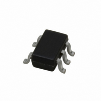
LMV7291MGX/NOPB National Semiconductor, LMV7291MGX/NOPB Datasheet - Page 12

LMV7291MGX/NOPB
Manufacturer Part Number
LMV7291MGX/NOPB
Description
IC COMPARATOR 1.8V R-R LP SC70-5
Manufacturer
National Semiconductor
Series
PowerWise®r
Type
General Purposer
Datasheet
1.LMV7291MGNOPB.pdf
(14 pages)
Specifications of LMV7291MGX/NOPB
Number Of Elements
1
Output Type
CMOS, Push-Pull, Rail-to-Rail
Voltage - Supply
1.8 V ~ 5 V, ±0.9 V ~ 2.5 V
Mounting Type
Surface Mount
Package / Case
6-TSSOP (5 lead), SC-88A, SOT-353
Lead Free Status / RoHS Status
Lead free / RoHS Compliant
Other names
LMV7291MGX
www.national.com
Application Notes
CIRCUIT TECHNIQUES FOR AVOIDING OSCILLATIONS
IN COMPARATOR APPLICATIONS
Feedback to almost any pin of a comparator can result in
oscillation. In addition, when the input signal is a slow volt-
age ramp or sine wave, the comparator may also burst into
oscillation near the crossing point. To avoid oscillation or
instability, PCB layout should be engineered thoughtfully.
Several precautions are recommended:
1. Power supply bypassing is critical, and will improve sta-
2. Keep all leads short to reduce stray capacitance and lead
3. It is a good practice to use an unbroken ground plane on
FIGURE 4. Non-Inverting Comparator with Hysteresis
bility and transient response. Resistance and inductance
from power supply wires and board traces increase
power supply line impedance. When supply current
changes, the power supply line will move due to its im-
pedance. Large enough supply line shift will cause the
comparator to mis-operate. To avoid problems, a small
bypass capacitor, such as 0.1uF ceramic, should be
placed immediately adjacent to the supply pins. An addi-
tional 6.8µF or greater tantalum capacitor should be
placed at the point where the power supply for the com-
parator is introduced onto the board. These capacitors
act as an energy reservoir and keep the supply imped-
ance low. In dual supply application, a 0.1µF capacitor is
recommended to be placed across V
inductance. It will also minimize any unwanted coupling
from any high-level signals (such as the output). The
comparators can easily oscillate if the output lead is
inadvertently allowed to capacitively couple to the inputs
via stray capacitance. This shows up only during the
output voltage transition intervals as the comparator
changes states. Try to avoid a long loop which could act
as an inductor (coil).
a printed circuit board to provide all components with a
(Continued)
+
and V
−
pins.
20080043
20080044
12
4. The output trace should be routed away from inputs. The
5. When the signal source is applied through a resistive
6. All pins of any unused comparators should be tied to the
Typical Applications
POSITIVE PEAK DETECTOR
A positive peak detect circuit is basically a comparator oper-
ated in a unity gain follower configuration, with a capacitor as
a load to maintain the highest voltage. A diode is added at
the output to prevent the capacitor from discharging through
the output, and a 1MΩ resistor added in parallel to the
capacitor to provide a high impedance discharge path. When
the input V
follows it, thus charging the capacitor. When it decreases,
the cap discharges through the 1MΩ resistor. The decay
time can be modified by changing the resistor. The output
should be accessed through a follower circuit to prevent
loading.
NEGATIVE PEAK DETECTOR
For the negative detector, the output transistor of the com-
parator acts as a low impedance current sink. Since there is
no pull-up resistor, the only discharge path will be the 1MΩ
resistor and any load impedance used. Decay time is
changed by varying the 1MΩ resistor.
low inductive ground connection. Make sure ground
paths are low-impedance where heavier currents are
flowing to avoid ground level shift. Preferably there
should be a ground plane under the component.
ground plane should extend between the output and
inputs to act as a guard.
network to one input of the comparator, it is usually
advantageous to connect the other input with a resistor
with the same value, for both DC and AC consideration.
Input traces should be laid out symmetrically if possible.
negative supply.
IN
FIGURE 5. Positive Peak Detector
increases, the inverting input of the comparator
20080054


