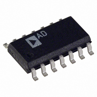
CMP04FS Analog Devices Inc, CMP04FS Datasheet - Page 2

CMP04FS
Manufacturer Part Number
CMP04FS
Description
IC COMPARATOR QUAD LP 14-SOIC
Manufacturer
Analog Devices Inc
Type
General Purposer
Datasheet
1.CMP04FSZ.pdf
(8 pages)
Specifications of CMP04FS
Mounting Type
Surface Mount
Output Type
CMOS, DTL, ECL, MOS, Open-Collector, TTL
Rohs Status
RoHS non-compliant
Number Of Elements
4
Voltage - Supply
3.3 V ~ 36 V, ±1.65 V ~ 18 V
Package / Case
14-SOIC (0.154", 3.90mm Width)
Comparator Type
Precision
No. Of Comparators
4
Response Time
1.3µs
Supply Voltage Min
3.3V
Peak Reflow Compatible (260 C)
No
Current Rating
0.8mA
Lead Free Status / RoHS Status
Contains lead / RoHS non-compliant
Available stocks
Company
Part Number
Manufacturer
Quantity
Price
Part Number:
CMP04FSZ
Manufacturer:
ADI/亚德诺
Quantity:
20 000
Company:
Part Number:
CMP04FSZ-REEL
Manufacturer:
AD
Quantity:
6 219
ABSOLUTE MAXIMUM RATINGS
Supply Voltage . . . . . . . . . . . . . . . . . . . . . . . . +36 V or ± 18 V
Differential Input Voltage . . . . . . . . . . . . . . . . . . . . . . 36 V dc
Input Voltage . . . . . . . . . . . . . . . . . . . . . . . . . –0.3 V to +36 V
Operating Temperature Range
Junction Temperature (T
Storage Temperature Range . . . . . . . . . . . . –65°C to +150°C
Input Current (V
Output Short Circuit to GND . . . . . . . . . . . . . . . . Continuous
Lead Temperature (Soldering, 60 sec) . . . . . . . . . . . . . 300°C
CMP04–SPECIFICATIONS
ELECTRICAL CHARACTERISTICS
Parameter
Input Offset Voltage
Input Offset Current
Input Bias Current
Voltage Gain
Large Signal Response Time
Small Signal Response Time
Input Voltage Range
Common-Mode Rejection Ratio
Power Supply Rejection Ratio
Saturation Voltage
Output Sink Current
Output Leakage Current
Supply Current
NOTES
1
2
3
4
5
Specifications subject to change without notice.
CAUTION
ESD (electrostatic discharge) sensitive device. Electrostatic charges as high as 4000 V readily
accumulate on the human body and test equipment and can discharge without detection. Although
the CMP04 features proprietary ESD protection circuitry, permanent damage may occur on
devices subjected to high energy electrostatic discharges. Therefore, proper ESD precautions are
recommended to avoid performance degradation or loss of functionality.
At output switch point, V
Guaranteed by design.
Sample tested.
The input common-mode voltage or input signal voltage should not be allowed to go negative by more than 0.3 V. The upper end of the common-mode voltage range
R
is V+ – 1.5 V, but either or both inputs can go to 30 V without damage.
CMP04FS . . . . . . . . . . . . . . . . . . . . . . . . . –40°C to +85°C
L
≥ 15 kΩ, V+ = 15 V, V
IN
< –3.0 V) . . . . . . . . . . . . . . . . . . . 50 mA
Model
CMP04FS
O
CM
= 1.4 V, R
= 1.5 V to 13.5 V.
J
) . . . . . . . . . . . . . –65°C to +150°C
S
= 0 Ω with V+ from 5 V, and over the full input common-mode range (0 V to V+ – 1.5 V).
Symbol
V
I
I
A
t
t
CMVR
CMRR
PSRR
V
I
I
I+
OS
B
r
r
SINK
LEAK
OS
OL
V
1
T
V
1 mV
OS
A
= 25 C
Conditions
R
I
I
R
V
V
V
V
Note 4
Notes 2, 5
V+ = 5 V to 18 V
V
V
V
R
(@ V+ = 5 V, T
IN
IN
IN
RL
IN
RL
IN
IN
IN
S
L
L
(+) – I
(+) or I
= 0 Ω, R
=
≥ 15 kΩ, V+ = 15 V
(–) ≥ 1 V, V
(–) ≥ 1 V, V
(+) ≥ 1 V, V
= TTL Logic Swing, V
= 100 mV Step
= 5 V, R
= 5 V, R
∞
Temperature
Ranges
–40°C to +85°C
ORDERING GUIDE
, All Comps V+ = 30 V
IN
IN
(–), R
L
(–)
L
L
= 5.1 kΩ, V
A
= 5.1 kΩ
= 5.1 kΩ
= 25 C, unless otherwise noted.)
IN
IN
–2–
IN
L
(+) = 0, I
(+) = 0, V
2
(–) = 0, V
= 5.1 kΩ, V
3
Package Type
14-Lead SOIC
NOTES
1
2
, 5 mV Overdrive
Absolute maximum ratings apply to both DICE and packaged parts, unless
θ
otherwise noted. Stresses above those listed under Absolute Maximum Ratings
may cause permanent damage to the device. This is a stress rating only; functional
operation of the device at these or any other conditions above those listed in the
operational sections of this specification is not implied. Exposure to absolute
maximum rating conditions for extended periods may affect device reliability.
soldered to printed circuit board for SOIC package.
JA
is specified for worst-case mounting conditions, i.e., θ
2
O
SINK
Package
Descriptions
14-Lead SOIC
REF
= 1.4 V
O
O
≤ 1.5 V
= 30 V
O
= 1.4 V
≤ 4 mA
= 1.4 V
1
3
Min
80
0
80
80
6
Package
Options
R-14
120
JA
WARNING!
Typ
0.4
2
25
200
300
1.3
100
100
250
16
0.1
0.8
2
ESD SENSITIVE DEVICE
Max
1
10
100
V+ – 1.5
400
100
2.0
36
JA
JC
is specified for device
REV. D
Unit
mV
nA
nA
V/mV
ns
µs
V
dB
dB
mV
mA
nA
mA
Unit
°C/W


