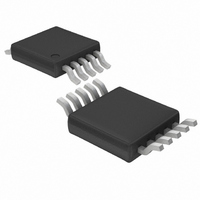
LT1715CMS Linear Technology, LT1715CMS Datasheet - Page 15

LT1715CMS
Manufacturer Part Number
LT1715CMS
Description
IC COMPARATOR 150MHZ DUAL 10MSOP
Manufacturer
Linear Technology
Series
UltraFast™r
Type
General Purposer
Datasheet
1.LT1715CMS.pdf
(20 pages)
Specifications of LT1715CMS
Number Of Elements
2
Output Type
CMOS, Rail-to-Rail, TTL
Voltage - Supply
2.7 V ~ 12 V
Mounting Type
Surface Mount
Package / Case
10-TFSOP, 10-MSOP (0.118", 3.00mm Width)
Lead Free Status / RoHS Status
Contains lead / RoHS non-compliant
Available stocks
Company
Part Number
Manufacturer
Quantity
Price
Company:
Part Number:
LT1715CMS
Manufacturer:
LT
Quantity:
10 000
Part Number:
LT1715CMS
Manufacturer:
LINEAR/凌特
Quantity:
20 000
Part Number:
LT1715CMS#PBF
Manufacturer:
LINEAR/凌特
Quantity:
20 000
Part Number:
LT1715CMS#TRPBF
Manufacturer:
LINEAR/凌特
Quantity:
20 000
Part Number:
LT1715CMS10
Manufacturer:
LINEAR/凌特
Quantity:
20 000
APPLICATIONS INFORMATION
ECL, and particularly PECL, is valuable technology for high
speed system design, but it must be used with care. With
less than a volt of swing, the noise margins need to be
evaluated carefully. Note that there is some degradation of
noise margin due to the ±5% resistor selections shown.
With 10KH/E, there is no temperature compensation of
the logic levels, whereas the LT1715 and the circuits
shown give levels that are stable with temperature. This
will lower the noise margin over temperature. In some
confi gurations it is possible to add compensation with
diode or transistor junctions in series with the resistors
of these networks.
For more information on ECL design, refer to the ECLiPS
data book (DL140), the 10KH system design handbook
(HB205) and PECL design (AN1406), all from Motorola,
now ON Semiconductor.
Circuit Description
The block diagram of the LT1715 is shown in Figure 9.
The circuit topology consists of a differential input stage,
again stage with hysteresis and a complementary com-
mon-emitter output stage. All of the internal signal paths
utilize low voltage swings for high speed at low power.
+IN
–IN
+
–
A
V1
V
V
CC
EE
+
Σ
+
Σ
Figure 9. LT1715 Block Diagram
NONLINEAR STAGE
+
–
A
V2
The input stage topology maximizes the input dynamic
range available without requiring the power, complexity
and die area of two complete input stages such as are
found in rail-to-rail input comparators. With a single
2.7V supply, the LT1715 still has a respectable 1.6V of
input common mode range. The differential input volt-
age rangeis rail-to-rail, without the large input currents
found incompeting devices. The input stage also features
phase reversal protection to prevent false outputs when
the inputs are driven below the –100mV common mode
voltage limit.
The internal hysteresis is implemented by positive, nonlin-
ear feedback around a second gain stage. Until this point,
the signal path has been entirely differential. The signal
path is then split into two drive signals for the upper and
lower output transistors. The output transistors are con-
nected common emitter for rail-to-rail output operation.
The Schottky clamps limit the output voltages at about
300mV from the rail, not quite the 50mV or 15mV of Linear
Technology’s rail-to-rail amplifiers and other products. But
the output of a comparator is digital, and this output stage
can drive TTL or CMOS directly. It can also drive ECL, as
described earlier, or analog loads.
+
–
+
–
1715 F09
+V
OUT
GND
S
LT1715
15
1715fa


