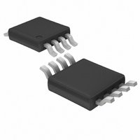
LT1711CMS8#TR Linear Technology, LT1711CMS8#TR Datasheet - Page 2

LT1711CMS8#TR
Manufacturer Part Number
LT1711CMS8#TR
Description
IC COMP R-RINOUT SINGLE 8-MSOP
Manufacturer
Linear Technology
Series
UltraFast™r
Type
General Purposer
Datasheet
1.LT1711CMS8PBF.pdf
(12 pages)
Specifications of LT1711CMS8#TR
Number Of Elements
1
Output Type
CMOS, Complementary, Rail-to-Rail, TTL
Voltage - Supply
2.4 V ~ 12 V, ±2.4 V ~ 6 V
Mounting Type
Surface Mount
Package / Case
8-TSSOP, 8-MSOP (0.118", 3.00mm Width)
Lead Free Status / RoHS Status
Contains lead / RoHS non-compliant
Other names
LT1711CMS8TR
Available stocks
Company
Part Number
Manufacturer
Quantity
Price
PACKAGE/ORDER I FOR ATIO
ABSOLUTE AXI U RATI GS
LT1711/LT1712
Supply Voltage
Differential Input Voltage ................................... 12.6V
Latch Pin Voltage ...................................................... 7V
Input and Latch Current ..................................... 10mA
Consult factory for parts specified with wider operating temperature ranges.
ELECTRICAL CHARACTERISTICS
The
V
SYMBOL PARAMETER
V
V
I
I
V
CMRR
PSRR
2
OS
B
OS
CM
+
V
+
OS
V
V
V
= 2.7V or V
/ T Input Offset Voltage Drift
+
+
–
+
T
JMAX
denotes specifications which apply over the full operating temperature range, otherwise specifications are at T
to V
to GND ........................................................ 12.6V
to GND .............................................– 10V to 0.3V
+IN
–IN
V
V
+
–
= 150 C,
Positive Supply Voltage Range
Input Offset Voltage (Note 4)
Input Offset Current
Input Bias Current (Note 5)
Input Voltage Range (Note 9)
Common Mode Rejection Ratio
Positive Power Supply Rejection Ratio
8-LEAD PLASTIC MSOP
–
1
2
3
4
............................................................ 12.6V
MS8 PACKAGE
+
TOP VIEW
= 5V, V
JA
= 250 C/ W (NOTE 12)
W
–
= 0V, V
8
7
6
5
Q
Q
GND
LATCH
ENABLE
W W
CM
U
= V
+
/2, V
MS8 PART MARKING
LATCH
ORDER PART
LT1711CMS8
LT1711IMS8
W
NUMBER
CONDITIONS
R
R
R
R
V
V
V
V
2.4V V
U
LTTC
LTTD
= 0.8V, C
S
S
S
S
+
+
+
+
= 50 , V
= 50 , V
= 50 , V
= 50 , V
= 5V, 0V V
= 5V, 0V V
= 2.7V, 0V V
= 2.7V, 0V V
+
U
LOAD
CM
CM
CM
CM
7V, V
(Note 1)
= V
= V
= 0V
= V
CM
CM
CM
CM
CM
= 10pF, V
+
+
+
/2
/2
= 0V
5V
5V
Output Current (Continuous) .............................. 20mA
Operating Temperature Range ................ – 40 C to 85 C
Specified Temperature Range (Note 2) ... – 40 C to 85 C
Junction Temperature .......................................... 150 C
Storage Temperature Range ................. – 65 C to 150 C
Lead Temperature (Soldering, 10 sec).................. 300 C
2.7V
2.7V
–IN A
+IN A
+IN B
–IN B
T
JMAX
V
V
V
V
OVERDRIVE
–
+
+
–
= 150 C,
16-LEAD PLASTIC SSOP
1
2
3
4
5
6
7
8
GN PACKAGE
TOP VIEW
JA
= 20mV, unless otherwise specified.
= 120 C/ W (NOTE 12)
16
15
14
13
12
11
10
9
LATCH
ENABLE A
GND
Q A
Q A
Q B
Q B
GND
LATCH
ENABLE B
– 0.1
MIN
– 18
– 35
2.4
56
53
54
50
58
56
GN PART MARKING
TYP
0.5
0.7
0.2
– 5
10
65
65
75
1
ORDER PART
LT1712CGN
LT1712IGN
NUMBER
A
1712
1712I
V
= 25 C.
+
MAX
5.0
6.0
10
+ 0.1
7
3
6
5
UNITS
V/ C
mV
mV
mV
mV
dB
dB
dB
dB
dB
dB
V
A
A
A
A
V


