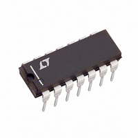
LT319AN Linear Technology, LT319AN Datasheet - Page 3

LT319AN
Manufacturer Part Number
LT319AN
Description
IC COMPARATOR DUAL 14-DIP
Manufacturer
Linear Technology
Type
General Purposer
Datasheet
1.LT319ANPBF.pdf
(12 pages)
Specifications of LT319AN
Number Of Elements
2
Output Type
Open-Collector, Open-Emitter, TTL
Voltage - Supply
5 V ~ 30 V, ±2.5 V ~ 15 V
Mounting Type
Through Hole
Package / Case
14-DIP (0.300", 7.62mm)
Lead Free Status / RoHS Status
Contains lead / RoHS non-compliant
Available stocks
Company
Part Number
Manufacturer
Quantity
Price
Part Number:
LT319AN#PBF
Manufacturer:
LINEAR/凌特
Quantity:
20 000
ELECTRICAL CHARACTERISTICS
The denotes the specifications which apply over the full operating temperature range, otherwise specifications are at T
Note 1: Absolute Maximum Ratings are those values beyond which the life
of a device may be impaired.
Note 2: For supply voltages less than 15V, the maximum input voltage is
equal to the supply voltage.
Note 3: Unless otherwise noted, supply voltage equals 15V and
V
voltage allowed between the ground pin and V
ground pin to V
voltage, offset current and bias current specifications apply for all supply
voltages between 15V and 5V unless otherwise specified.
SYMBOL PARAMETER
V
I
SYMBOL PARAMETER
V
CMRR
I
I
A
V
I
temperature range, otherwise specifications are at T
S
OS
B
S
CM
SAT
OS
V
SAT
= 0V, T
Saturation Voltage
Output Leakage Current
Input Voltage Range
Differential Input Voltage
Supply Current
Positive Supply Current
Negative Supply Current
Input Offset Voltage
Common Mode Rejection Ratio
Input Offset Current
Input Bias Current
Voltage Gain
Response Time
Saturation Voltage
Output Leakage Current
Input Voltage Range
Differential Input Voltage
Supply Current
Positive Supply Current
Negative Supply Current
A
= 25 C. The ground pin is grounded. Note that the maximum
–
when the power supply voltage exceeds 9V. The offset
+
(Note 5)
CONDITIONS
V
V
V
V
V
V
V
V
V
CONDITIONS
V
R
(Note 4)
(Note 4)
(Note 4)
V
V
V
V
V
V
V
V
V
T
T
is 18V. Do not tie the
IN
+
IN
IN
S
S
S
S
IN
IN
IN
S
+
S
S
+
+
S
+
+
A
A
= 15V
= 5V, V
= 5V, V
= 15V
= 15V
= 15V, V
= 15V
= 5V, V
= 5V, V
= 15V
= 15V
4.5V, V
4.5V, V
5k
5mV, V
10mV, V
–5mV, I
–6mA, I
–10mV, I
–10mV, I
0 C
0 C
–
–
–
–
= 0V
= 0V
= 0V
= 0V
–
–
CM
OUT
O
SINK
= 0V
A
= 0V,
OUT
SINK
SINK
= 25mA,
= 25 C. (Note 3)
= 0V
to V
to V
= 25mA
3.2mA
–
The
3.2mA
–
= 35V
= 35V
denotes the specifications which apply over the full operating
Note 4: The offset voltages and currents given are the maximum values
required to drive the output within 1V of either supply with a 1mA load,
thus these parameters define an error band and take into account the
worst case effects of voltage gain and input impedance.
Note 5: Response time specified is for a 100mV input step with 5mV
overdrive.
Note 6: Inputs are protected with back-to-back 5.6V zener diodes. This
limits maximum differential input voltage to 5V if current is unlimited.
Larger differential input drive is allowed if input current is limited to 5mA
with external resistance.
MIN
MIN
–12
90
20
1
1
LT119A
LT319A
0.75
0.23
0.75
TYP
TYP
106
150
0.2
4.3
0.3
0.5
0.3
0.2
4.3
30
40
80
1
13
8
3
13
8
3
1000
MAX
MAX
11.5
12.5
500
1.5
0.4
0.6
4.5
0.5
1.5
0.4
10
12
40
60
10
2
3
1
2
3
5
5
5
LT119A/LT319A
MIN
MIN
–12
LM119/LM319
1
1
8
LM119
LM319
0.75
0.23
0.75
TYP
TYP
250
0.2
4.3
0.3
0.2
4.3
80
80
40
1
13
8
3
2
13
8
3
A
1000
1200
MAX
MAX
11.5
= 25 C. (Note 3)
12.5
200
300
1.5
0.4
0.6
4.5
1.5
0.4
10
12
10
10
2
3
8
8
3
5
5
5
119a319afb
UNITS
UNITS
V/mV
3
mA
mA
mA
mV
mV
mV
mA
mA
mA
dB
nA
nA
nA
nA
ns
V
V
V
A
A
V
V
V
V
V
A
V
V
V


