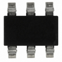
LT1719CS6#TRMPBF Linear Technology, LT1719CS6#TRMPBF Datasheet - Page 4

LT1719CS6#TRMPBF
Manufacturer Part Number
LT1719CS6#TRMPBF
Description
IC COMP R-RINOUT SINGLE SOT23-6
Manufacturer
Linear Technology
Series
UltraFast™r
Type
General Purposer
Specifications of LT1719CS6#TRMPBF
Number Of Elements
1
Output Type
CMOS, Rail-to-Rail, TTL
Voltage - Supply
2.7 V ~ 6 V
Mounting Type
Surface Mount
Package / Case
SOT-23-6
Comparator Type
General Purpose
No. Of Comparators
1
Response Time
4.5ns
Ic Output Type
CMOS, TTL
Output Compatibility
CMOS, TTL
Supply Current
4.6mA
Supply Voltage Range
2.7V To 6V
Rohs Compliant
Yes
Lead Free Status / RoHS Status
Lead free / RoHS Compliant
Other names
LT1719CS6#TRMPBFTR
Available stocks
Company
Part Number
Manufacturer
Quantity
Price
LT1719
ELECTRICAL CHARACTERISTICS
SYMBOL PARAMETER
I
I
I
I
I
I
I
I
I
I
I
I
Note 1: Stresses beyond those listed under Absolute Maximum Ratings
may cause permanent damage to the device. Exposure to any Absolute
Maximum Rating condition for extended periods may affect device
reliability and lifetime.
Note 2: If one input is within these common mode limits, the other input
can go outside the common mode limits and the output will be valid.
Note 3: The LT1719 comparator includes internal hysteresis. The trip
points are the input voltage needed to change the output state in each
direction. The offset voltage is defi ned as the average of V
while the hysteresis voltage is the difference of these two.
Note 4: The LT1719S8 common mode rejection ratio is measured with
V
from V
Note 5: The LT1719S6 common mode rejection ratio is measured with
V
V
Note 6: The LT1719S8 power supply rejection ratio is measured with
V
4
temperature range, otherwise specifi cations are at T
LT1719S8 V
S
+
SHDN5
SHDN3
CCS
SS
EES
+
CCSO
SSO
EEO
+
CC
+
CM
CM
S
O
= 5V and is defi ned as the change in offset voltage measured from
= 5V, V
= –0.1V to V
= 1V and is defi ned as the worst of: the change in offset voltage from
CM
= –5.1V to V
EE
Positive Output Stage Supply Current
Supply Current
Shutdown Pin Current
Shutdown Pin Current
Disabled Supply Currents (LT1719S8)
= – 5V and is defi ned as the change in offset voltage measured
CC
= +V
CM
= 3.8V, divided by 3.9V.
S
CM
= 5V and V
= 3.8V, divided by 8.9V.
(LT1719S8 Only) V
EE
(LT1719S6) V
(LT1719S8)
(LT1719S8)
(LT1719S6)
(LT1719S8)
(LT1719S8)
(LT1719S8)
(LT1719S6)
= –5V, for the LT1719S6 V
CONDITIONS
+ V
V
+V
+V
+ V
V
V
+ V
Shutdown Pin Open
V
S
+
+
SHDN
+
+
S
S
S
= 5V
= 3V
S
= 6V, V
S
= 6V, Shutdown Pin Open
= V
or V
or V
= V
= 6V, V
= 6V, V
TRIP
CC
= +V
A
CC
+
+
+
= 3V, V
= 25°C. V
SHDN
= 5V
= 3V
and V
= 5V, V
CC
S
CC
– 0.5V
= 5V, V
= 5V, V
The
= +V
+
TRIP
EE
= 5V, V
EE
= 0V
S
–
l
= –5V
CM
,
EE
EE
– 0.5V
denotes the specifi cations which apply over the full operating
= –5V
= –5V
= 1V, V
–
= 0V, unless otherwise specifi ed.
V
from V
Note 7: The LT1719S6 power supply rejection ratio is measured with
V
V
Note 8: Because of internal hysteresis, there is no small-signal region in
which to measure gain. Proper operation of internal circuity is ensured by
measuring V
Note 9: Propagation delay measurements made with 100mV steps.
Overdrive is measured relative to V
Note 10: t
low values of overdrive. The LT1719 is 100% tested with a 100mV step
and 20mV overdrive. Correlation tests have shown that t
guaranteed with this test, if additional DC tests are performed to guarantee
that all internal bias conditions are correct.
Note 11: Propagation Delay Skew is defi ned as:
EE
CM
+
= 2.7V to V
= – 5.5V to V
SHDN
= 1V and is defi ned as the change in offset voltage measured from
CC
= +V
PD
t
= 0.5V, V
SKEW
OH
cannot be measured in automatic handling equipment with
+
S
= 6V, divided by 3.3V.
and V
= 2.7V to V
EE
= |t
= 0V divided by 5.5V, or the change in offset voltage
PDLH
OVERDRIVE
OL
with only 10mV of overdrive.
– t
CC
PDHL
l
l
l
l
l
l
l
l
l
l
l
l
l
l
= +V
= 20mV, C
|
S
TRIP
–300
–200
MIN
–30
–20
= 6V (with V
±
.
OUT
–110
–0.2
TYP
–80
4.2
3.3
4.6
4.2
0.2
0.1
0.1
0.1
0.2
7
7
= 10pF and for the
EE
= 0V) divided by 3.3V.
PD
MAX
–30
–20
30
50
80
20
20
40
8
6
9
7
limits can be
UNITS
1719fa
mA
mA
mA
mA
μA
μA
μA
μA
μA
μA
μA
μA
μA
μA


