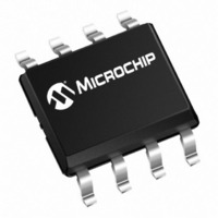
MCP6541T-I/MS Microchip Technology, MCP6541T-I/MS Datasheet - Page 13

MCP6541T-I/MS
Manufacturer Part Number
MCP6541T-I/MS
Description
IC COMP PUSHPULL 1.6V SNGL 8MSOP
Manufacturer
Microchip Technology
Type
General Purposer
Specifications of MCP6541T-I/MS
Output Type
CMOS, Push-Pull, Rail-to-Rail, TTL
Package / Case
8-TSSOP, 8-MSOP (0.118", 3.00mm Width)
Number Of Elements
1
Voltage - Supply
1.6 V ~ 5.5 V
Mounting Type
Surface Mount
Number Of Channels
1 Channel
Product
Analog Comparators
Response Time
4 us
Offset Voltage (max)
5 mV
Input Bias Current (max)
1 pA
Supply Voltage (max)
5.5 V
Supply Voltage (min)
1.6 V
Supply Current (max)
1 mA
Maximum Operating Temperature
+ 85 C
Mounting Style
SMD/SMT
Minimum Operating Temperature
- 40 C
Lead Free Status / RoHS Status
Lead free / RoHS Compliant
Other names
MCP6541TI/MS
Where:
Using this simplified circuit, the trip voltage can be
calculated using the following equation:
EQUATION
Figure 2-19 and Figure 2-22 can be used to determine
typical values for V
3.5
With this family of comparators, the power supply pin
(V
capacitor (i.e., 0.01 µF to 0.1 µF) within 2 mm for good
edge rate performance.
3.6
Reasonable capacitive loads (e.g., logic gates) have
little impact on propagation delay (see Figure 2-27).
The supply current increases with increasing toggle
frequency
capacitive loads.
3.7
In order to maximize battery life in portable
applications, use large resistors and small capacitive
loads. Also, avoid toggling the output more than
necessary and do not use chip select (CS) to conserve
power for short periods of time. Capacitive loads will
draw additional power at start-up.
V
V
2003 Microchip Technology Inc.
DD
TLH
THL
for single supply) should have a local bypass
= trip voltage from low to high
= trip voltage from high to low
V
V
THL
TLH
Bypass Capacitors
Capacitive Loads
Battery Life
(Figure 2-30),
=
=
V
V
V
OH
OL
23
OH
R
---------------------- -
R
---------------------- -
R
=
23
23
23
and V
R
------------------
R
R
=
+
+
23
23
2
R
+
R F
R F
------------------
R
3
R
OL
2
R
especially
2
+
3
R
.
+
+
R
3
3
V
V
V
DD
23
23
--------------------- -
R
--------------------- -
R
23
23
R
R
+
with
+
F
F
R
R
F
F
higher
3.8
In applications where low input bias current is critical,
PCB (Printed Circuit Board) surface leakage effects
need to be considered. Surface leakage is caused by
humidity, dust or other contamination on the board.
Under low humidity conditions, a typical resistance
between nearby traces is 10
cause 5 pA, if current-to-flow. This is greater than the
MCP6541/2/3/4 family’s bias current at 25°C (1 pA,
typ).
The easiest way to reduce surface leakage is to use a
guard ring around sensitive pins (or traces). The guard
ring is biased at the same voltage as the sensitive pin.
An example of this type of layout is shown in
Figure 3-8.
FIGURE 3-8:
for Inverting Circuit.
1.
2.
Inverting Configuration (Figures 3-5 and 3-8):
a.
b.
Non-inverting Configuration (Figure 3-3):
a.
b.
PCB Surface Leakage
Connect the guard ring to the non-inverting
input pin (V
to the same reference voltage as the
comparator (e.g., V
Connect the inverting pin (V
pad without touching the guard ring.
Connect the non-inverting pin (V
input pad without touching the guard ring.
Connect the guard ring to the inverting input
pin (V
IN
MCP6541/2/3/4
–).
V
IN
IN
Guard Ring
+). This biases the guard ring
Example Guard Ring Layout
-
12
DD
/2 or ground).
. A 5V difference would
V
IN
+
DS21696C-page 13
IN
–) to the input
IN
V
+) to the
SS


