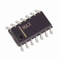
MAX9202ESD+ Maxim Integrated Products, MAX9202ESD+ Datasheet - Page 6

MAX9202ESD+
Manufacturer Part Number
MAX9202ESD+
Description
IC COMPARATOR LP 14-SOIC
Manufacturer
Maxim Integrated Products
Type
with Latchr
Datasheet
1.MAX9203ESA.pdf
(8 pages)
Specifications of MAX9202ESD+
Number Of Elements
2
Output Type
TTL
Voltage - Supply
4.75 V ~ 10.5 V, ±2.375 V ~ 5.75 V
Mounting Type
Surface Mount
Package / Case
14-SOIC (0.154", 3.90mm Width)
Number Of Channels
2 Channels
Supply Voltage (max)
10.5 V
Supply Voltage (min)
4.75 V
Supply Current (max)
4 mA
Maximum Operating Temperature
+ 85 C
Mounting Style
SMD/SMT
Minimum Operating Temperature
- 40 C
Propagation Delay Time
7 ns
Comparator Type
High Speed
No. Of Comparators
2
Response Time
7ns
Ic Output Type
TTL
Supply Current
2.5mA
Supply Voltage Range
5V To 10V, ± 4.75V To ± 5.25V
Amplifier Case Style
SOIC
Rohs Compliant
Yes
Lead Free Status / RoHS Status
Lead free / RoHS Compliant
Figure 1a. Separate Analog Supply,
Common Ground
MAX9203
6
Low Cost, 7ns, Low-Power
Voltage Comparators
Because of the large gain-bandwidth transfer function
of the MAX9201/MAX9202/MAX9203 special precau-
tions must be taken to realize their full high-speed
capability. A printed circuit board with a good, low-
inductance ground plane is mandatory. All decoupling
capacitors (the small 100nF ceramic type is a good
choice) should be mounted as close as possible to the
power-supply pins. Separate decoupling capacitors for
analog V
Close attention should be paid to the bandwidth of the
SO
_______________________________________________________________________________________
1
2
3
4
5
6
7
8
PIN
CC
SOT
Pin Description (continued)
8
7
6
5
4
3
2
1
and for digital V
+10V
V
V
Applications Information
CC
EE
+5V
LATCH
NAME
GND
OUT
V
V
IN+
V
GND
V
IN-
CC
DD
DD
EE
DD
FUNCTION
Positive Analog Supply
Positive Input
Negative Input
Negative Analog Supply and
Substrate
Latch Input
Ground
Output
Positive Digital Supply
OUT
are also recommended.
Circuit Layout
Figure 1b. Single +5V Supply, Common
Ground
V
V
+5V
CC
EE
decoupling and terminating components. Short lead
lengths on the inputs and outputs are essential to avoid
unwanted parasitic feedback around the comparators.
Solder the device directly to the printed circuit board
instead of using a socket.
As with all high-speed comparators, the high gain-band-
width product of the MAX9201/MAX9202/ MAX9203 can
create oscillation problems when the input traverses the
linear region. For clean output switching without oscilla-
tion or steps in the output waveform, the input must meet
minimum slew-rate requirements (0.5V/s typ). Oscillation
is largely a function of board layout and of coupled
source impedance and stray input capacitance. Both
poor layout and large source impedance will cause the
part to oscillate and increase the minimum slew-rate
requirement. In some applications, it may be helpful to
apply some positive feedback between the output and
positive input. This pushes the output through the transi-
tion region clearly, but applies a hysteresis in threshold
seen at the input terminals.
The comparator TTL output stages are optimized for
driving low-power Schottky TTL with a fan-out of four.
When the latch is connected to a logic high level, the
comparator is transparent and immediately responds to
changes at the input terminals. When the latch is con-
nected to a TTL low level, the comparator output latch-
es (in the same state) the instant that the latch
command is applied, and will not respond to subse-
quent changes at the input. No latch is provided on
the MAX9201.
Typical Power-Supply Alternatives
V
GND
DD
OUT
Input Slew-Rate Requirements
TTL Output and Latch Inputs
Figure 1c. Split ±5V Supply, Separate
Ground
+5V
-5V
V
V
CC
EE
+5V
GND
V
DD
OUT


