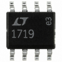
LT1719CS8#PBF Linear Technology, LT1719CS8#PBF Datasheet - Page 9

LT1719CS8#PBF
Manufacturer Part Number
LT1719CS8#PBF
Description
IC COMP R-R I/O SGL 3/5V 8-SOIC
Manufacturer
Linear Technology
Series
UltraFast™r
Type
General Purposer
Specifications of LT1719CS8#PBF
Number Of Elements
1
Output Type
CMOS, Rail-to-Rail, TTL
Voltage - Supply
2.7 V ~ 10.5 V
Mounting Type
Surface Mount
Package / Case
8-SOIC (0.154", 3.90mm Width)
Comparator Type
General Purpose
No. Of Comparators
1
Response Time
4.5ns
Ic Output Type
CMOS, TTL
Output Compatibility
CMOS, TTL
Supply Current
4.2mA
Supply Voltage Range
2.7V To 10.5V
Rohs Compliant
Yes
Lead Free Status / RoHS Status
Lead free / RoHS Compliant
Available stocks
Company
Part Number
Manufacturer
Quantity
Price
APPLICATIONS INFORMATION
Power Supply Confi gurations (SO-8 Package)
The LT1719S8 has separate supply pins for the input and
output stages that allow fl exible operation, accommodating
separate voltage ranges for the analog input and the output
logic. Of course, a single 3V/5V supply may be used by
tying + V
The minimum voltage requirement can be simply stated
as both the output and the input stages need at least 2.7V
and the V
The following rules must be adhered to in any
confi guration:
Although the ground pin need not be tied to system ground,
most applications will use it that way. Figure 1 shows three
common confi gurations. The fi nal one is uncommon, but
it will work and may be useful as a level translator; the
input stage is run from – 5.2V and ground while the output
stage is run from 3V and ground. In this case the com-
mon mode input voltage range does not include ground,
so it may be helpful to tie V
V
rules are not violated.
Input Voltage Considerations
The LT1719 is specifi ed for a common mode range of
–100mV to 3.8V when used with a single 5V supply. A
more general consideration is that the common mode
range is 100mV below V
criterion for this common mode limit is that the output still
responds correctly to a small differential input signal. If
one input is within the common mode limit, the other
input signal can go outside the common mode limits, up
to the absolute maximum limits, and the output will retain
the correct polarity.
CC
2.7V ≤ (V
2.7V ≤ (+ V
(+V
V
EE
may also be tied below ground, as long as the above
S
≤ Ground
– V
S
EE
and V
EE
pin must be equal to or less than ground.
CC
S
) ≤ 10.5V
– V
– GND) ≤ 6V
CC
together as well as GND and V
EE
) ≤ 10.5V
EE
/V
CC
–
to 3V anyway. Conversely,
to 1.2V below V
CC
/V
EE
+
.
. The
When either input signal falls below the negative com-
mon mode limit, the internal PN diode formed with the
substrate can turn on, resulting in signifi cant current
fl ow through the die. An external Schottky clamp diode
between the input and the negative rail can speed up re-
covery from negative overdrive by preventing the substrate
diode from turning on.
When both input signals are below the negative common
mode limit, phase reversal protection circuitry prevents
false output inversion to at least – 400mV common mode.
However, the offset and hysteresis in this mode will increase
dramatically, to as much as 15mV each. The input bias
currents will also increase.
When both input signals are above the positive common
mode limit, the input stage will get debiased and the output
polarity will be random. However, the internal hysteresis
will hold the output to a valid logic level. When at least one
of the inputs returns to within the common mode limits,
recovery from this state can take as long as 1μs.
Figure 1. Variety of SO-8 Power Supply Confi gurations
Single Supply
10V
+
–
10V
+
–
LT1719S8
LT1719S8
2.7V TO 6V
V
V
V
V
IN
CC
EE
CC
EE
, 5V
5V
OUT
+V
+V
GND
GND
S
S
Front End Entirely Negative
±5V
–5.2V
–
–
+
–5V
+
5V
LT1719S8
LT1719S8
V
V
V
V
IN
CC
EE
CC
EE
, 3V
LT1719
3V
OUT
3V
GND
GND
+V
+V
1719 F01
S
S
1719fa
9


