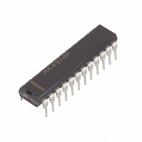
DS2167 Maxim Integrated Products, DS2167 Datasheet

DS2167
Specifications of DS2167
Available stocks
Related parts for DS2167
DS2167 Summary of contents
Page 1
... Ideal for voice mail applications • 28-pin surface-mount package available, designated DS2167Q/DS2168Q DESCRIPTION The DS2167 and DS2168 are dedicated digital signal processor (DSP) CMOS chips optimized for Adaptive Differential Pulse Code Modulation (ADPCM) based compression algorithms. The devices halve the trans- DS2167/DS2168 ...
Page 2
... DS2167/DS2168 PRODUCT OVERVIEW The DS2167 and DS2168 contain three major function- al blocks: a high performance (10 MIPS) DSP “engine,” two independent PCM data interfaces (“X” and “Y”) which connect directly to serial time division multiplexed (TDM) backplanes and a microcontroller-compatible serial port for on-the-fly device configuration. A 10MHz master clock is required by the DSP engine. The de- vices’ ...
Page 3
... HARDWARE RESET RST allows the user to reset both channel algorithms and register contents. This input must be held low for at least system power-up after master clock is stable to assure proper initialization of the device. RST DS2167/DS2168 DESCRIPTION for normal operation SS to select the serial port ...
Page 4
... When both X and Y sides are idled, the devices enter a stand-by mode which significantly reduces power consumption. 3. The DS2167 will power-up within 200 ms after the side is reactivated (SDI and/or CS not equal to 0) from standby. 4. The DS2168 must be hardware reset when reactivated from standby. Power-up occurs immediately after the reset ...
Page 5
... Codec/Filter devices can be substituted. SOFTWARE MODE Tying SPS high enabled the software mode. In this mode, a host microcontroller writes configuration data to the DS2167/DS2168 serial port via inputs SCLK, SDI, and CS. Independent control and timeslot registers es- tablish operating characteristics for the X-side and Y- side PCM interfaces. ...
Page 6
... DS2167/DS2168 both X and Y interfaces, the device enters a low-power standby mode. The DS2167 will power-up within 200 ms after the side is reactivated (IPD=0) from standby. The DS2168 requires an external hardware re- set after IPD is cleared to “wake-up” from standby. The DS2168 will power-up immediately after the low-high transition on RST ...
Page 7
... NAME AND DESCRIPTION – ITR.7 Reserved, must be 0 for proper operation. – ITR.6 Reserved, must be 0 for proper operation. D5 ITR.5 MSB of input timeslot word. D4 ITR.4 D3 ITR.3 D2 ITR.2 D1 ITR.1 D0 ITR.0 LSB of input timeslot word. DS2167/DS2168 (LSB) µ/A BYP – CP/EX (LSB 022698 7/15 ...
Page 8
... DS2167/DS2168 OUTPUT TIMESLOT REGISTER Figure 6 (MSB) – – SYMBOL POSITION NAME AND DESCRIPTION – OTR.7 Reserved, must be 0 for proper operation. – OTR.6 Reserved, must be 0 for proper operation. D5 OTR.5 MSB of output timeslot word. D4 OTR.4 D3 OTR.3 D2 OTR.2 D1 OTR.1 D0 OTR.0 LSB of output timeslot word. ...
Page 9
... VSS 10 MHz PCM DATA HI-WAY “Y” CLOCK PCM DATA HI-WAY “X” DS2167/DS2168 command and control) or four bytes (address/com- mand, control, input timeslot and output timeslot) in length. Writes should be terminated on byte boundaries to insure data integrity. PCM and ADPCM outputs will tristate during register updates. É ...
Page 10
... DS2167/DS2168 ABSOLUTE MAXIMUM RATINGS* Voltage on Any Pin Relative to Ground Operating Temperature Storage Temperature Soldering Temperature * This is a stress rating only and functional operation of the device at these or any other conditions above those indicated in the operation sections of this specification is not implied. Exposure to absolute maxi- mum rating conditions for extended periods of time may affect reliability ...
Page 11
... V = 0.8V, and 10 ns maximum rise and fall times Load = 150 LSTTL loads. 3. For LSB of PCM byte or ADPCM nibble. 4. Maximum width of FSX, FSY is one CLKX, CLKY period. 5. MCLK = 10 MHz + 500 ppm. DS2167/DS2168 (0°C to 70° 10%) DD MIN TYP MAX UNITS 100 ...
Page 12
... DS2167/DS2168 MASTER CLOCK/RESET AC ELECTRICAL CHARACTERISTICS PARAMETER SYMBOL MCLK Period t PM MCLK Pulse Width t , WMH t WML RST Pulse Width t WRL SERIAL PORT AC ELECTRICAL CHARACTERISTICS PARAMETER SYMBOL SDI to SCLK Setup t DC SCLK to SDI Hold t CDH SCLK Low Time t CL SCLK High Time t CH ...
Page 13
... RM MCLK t WRL RST SERIAL PORT WRITE AC TIMING DIAGRAM Figure SCC SCLK t DC É É É É É É É É É SDI É É É É É É É É É t CDH DS2167/DS2168 t PXY t FXY t t WXYH WXYL DXYZ DXYO WMH ...
Page 14
... DS2167/DS2168 DS2167/DS2168 ADPCM PROCESSOR 24-PIN DIP INCHES DIM MIN MAX A IN. 1.245 1.270 MM 31.62 32.25 B IN. 0.530 0.550 MM 13.46 13.97 C IN. 0.140 0.160 MM 3.56 4.06 D IN. 0.600 0.625 MM 15.24 15.88 E IN. 0.015 0.050 MM 0.380 1.27 F IN. 0.120 0.145 MM 3.05 3.68 G IN. ...
Page 15
... DS2167/DS2168Q ADPCM PROCESSOR 28-PIN PLCC CH1 e1 E2 INCHES DIM. MIN. MAX. A 0.165 0.180 A1 0.090 0.120 A2 0.020 – B 0.026 0.033 B1 0.013 0.021 C 0.009 0.012 D 0.485 0.495 D1 0.450 0.456 D2 0.390 0.430 E 0.485 0.495 E1 0.450 0.456 E2 0.390 0.430 L1 0.060 – – e1 0.050 BSC CH1 ...


