LM1973N/NOPB National Semiconductor, LM1973N/NOPB Datasheet - Page 3
LM1973N/NOPB
Manufacturer Part Number
LM1973N/NOPB
Description
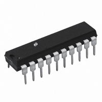
IC AUDIO ATTENUATOR 3CH 20-DIP
Manufacturer
National Semiconductor
Type
Audio Attenuatorr
Datasheet
1.LM1973MNOPB.pdf
(12 pages)
Specifications of LM1973N/NOPB
Applications
Consoles, MIDI
Mounting Type
Through Hole
Package / Case
20-DIP (0.300", 7.62mm)
Lead Free Status / RoHS Status
Lead free / RoHS Compliant
Other names
*LM1973N
*LM1973N/NOPB
LM1973N
*LM1973N/NOPB
LM1973N


Electrical Characteristics
Note 6: Limits are guaranteed to National’s AOQL (Average Output Quality Level).
Note 7: At the present time the Crosstalk measurement is specified as a typical only, which is due to a hardware limitation of the automated test equipment.
Timing Diagram
Pin Descriptions
Signal Ground (1, 5, 17): Each input has its own indepen-
dent ground, GND1, GND2, and GND3.
Signal Input (2, 4, 18): There are 3 independent signal
inputs, IN1, IN2, and IN3.
Signal Output (6, 16, 20): There are 3 independent signal
outputs, OUT1, OUT2, and OUT3.
Voltage Supply (13, 15): Positive voltage supply pins, V
and V
Voltage Supply (7, 19): Negative voltage supply pins, V
and V
tion.
AC Ground (3, 14): These two pins are not physically con-
nected to the die in any way (i.e., No bondwires). These pins
must be AC grounded to prevent signal coupling between
any of the pins nearby. Pin 14 should be connected to pins
13 and 15 for ease of wiring and the best isolation.
Logic Ground (8): Digital signal ground for the interface
lines; CLOCK, LOAD/SHIFT, DATA-IN and DATA-OUT.
Clock (9): The clock input accepts a TTL or CMOS level
signal. The clock input is used to load data into the internal
shift register on the rising edge of the input clock waveform.
Load/Shift (10): The load/shift input accepts a TTL or
CMOS level signal. This is the enable pin of the device,
allowing data to be clocked in while this input is low (0V).
Data-In (11): The data-in input accepts a TTL or CMOS level
signal. This pin is used to accept serial data from a micro-
controller that will be latched and decoded to change a
channel’s attenuation level.
DD2
SS2
. To be tied to ground in a single supply configura-
.
(Notes 1, 2) (Continued)
FIGURE 2. Timing Diagram
DD1
SS1
3
Data-Out (12): This pin is used in daisy-chain mode where
more than one µPot is controlled via the same data line. As
the data is clocked into the chain from the µC, the preceding
data in the shift register is shifted out the DATA-OUT pin to
the next µPot in the chain or to ground if it is the last µPot in
the chain. The LOAD/SHIFT line goes high once all of the
new data has been shifted into each of its respective regis-
ters.
Connection Diagram
01195802
www.national.com
01195803
Related parts for LM1973N/NOPB
Image
Part Number
Description
Manufacturer
Datasheet
Request
R

Part Number:
Description:
Micro-Pot 3-Channel 76 dB Audio Attenuator with Mute
Manufacturer:
National Semiconductor
Datasheet:
Part Number:
Description:
National Semiconductor [8-Bit D/A Converter]
Manufacturer:
National Semiconductor
Datasheet:
Part Number:
Description:
National Semiconductor [Media Coprocessor]
Manufacturer:
National Semiconductor
Datasheet:
Part Number:
Description:
Digitally Controlled Tone and Volume Circuit with Stereo Audio Power Amplifier, Microphone Preamp Stage and National 3D Sound
Manufacturer:
National Semiconductor
Datasheet:
Part Number:
Description:
Digitally Controlled Tone and Volume Circuit with Stereo Audio Power Amplifier, Microphone Preamp Stage and National 3D Sound
Manufacturer:
National Semiconductor
Datasheet:
Part Number:
Description:
AC97 Rev 2 Codec with Sample Rate Conversion and National 3D Sound
Manufacturer:
National Semiconductor
Part Number:
Description:
Manufacturer:
National Semiconductor
Datasheet:
Part Number:
Description:
Manufacturer:
National Semiconductor
Datasheet:
Part Number:
Description:
General Purpose, Low Voltage, Low Power, Rail-to-Rail Output Operational Amplifiers
Manufacturer:
National Semiconductor
Datasheet:
Part Number:
Description:
8-bit 20 MSPS flash A/D converter.
Manufacturer:
National Semiconductor
Datasheet:
Part Number:
Description:
Low Noise Quad Operational Amplifier
Manufacturer:
National Semiconductor
Datasheet:
Part Number:
Description:
Quad Differential Line Receivers
Manufacturer:
National Semiconductor
Datasheet:
Part Number:
Description:
Quad High Speed Trapezoidal? Bus Transceiver
Manufacturer:
National Semiconductor
Datasheet:
Part Number:
Description:
Dual Line Receiver
Manufacturer:
National Semiconductor
Datasheet: