NE570DG ON Semiconductor, NE570DG Datasheet
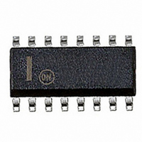
IC COMPANDOR DUAL GAIN 16-SOIC

NE570DG

Manufacturer Part Number
NE570DG
Description
IC COMPANDOR DUAL GAIN 16-SOIC
Manufacturer
ON Semiconductor
Type
Compandorr
Datasheet

Specifications of NE570DG

Applications
Cellular Radio, Players
Mounting Type
Surface Mount
Package / Case
16-SOIC (0.300", 7.5mm Width)
Operating Supply Voltage
9 V, 12 V, 15 V, 18 V
Supply Current
4.3 mA
Maximum Operating Temperature
+ 70 C
Mounting Style
SMD/SMT
Minimum Operating Temperature
0 C
Supply Type
Analog
Supply Voltage (max)
24 V
Supply Voltage (min)
6 V
Ic Function
Compandor
Brief Features
Compressor And Expander, Temperature Compensated
Supply Voltage Range
6V To 24V
Operating Temperature Range
0°C To +70°C
Digital Ic Case Style
SOIC
Rohs Compliant
Yes
Lead Free Status / RoHS Status
Lead free / RoHS Compliant

Available stocks

Company
Part Number
Manufacturer
Quantity
Price
Part Number:
NE570DG
Manufacturer:
ON
Quantity:
211
Part Number:
NE570DG
Manufacturer:
ON/安森美
Quantity:
20 000
NE570
Compandor
either channel may be used as a dynamic range compressor or
expandor. Each channel has a full−wave rectifier to detect the average
value of the signal, a linerarized temperature−compensated variable
gain cell, and an operational amplifier.
communications systems, modems, telephone, and satellite
broadcast/receive audio systems.
Features
Applications
Stresses exceeding Maximum Ratings may damage the device. Maximum
Ratings are stress ratings only. Functional operation above the Recommended
Operating Conditions is not implied. Extended exposure to stresses above the
Recommended Operating Conditions may affect device reliability.
*For additional information on our Pb−Free strategy and soldering details, please
May, 2006 − Rev. 4
MAXIMUM RATINGS
download the ON Semiconductor Soldering and Mounting Techniques
Reference Manual, SOLDERRM/D.
Maximum Operating Voltage
Operating Ambient Temperature Range
Operating Junction Temperature
Power Dissipation
Thermal Resistance, Junction−to−Ambient
The NE570 is a versatile low cost dual gain control circuit in which
The NE570 is well suited for use in cellular radio and radio
DG CELL IN
Complete Compressor and Expandor in One IC
Temperature Compensated
Greater than 110 dB Dynamic Range
Operates Down to 6.0 V
System Levels Adjustable with External Components
Distortion may be Trimmed Out
Pb−Free Packages are Available*
Cellular Radio
Telephone Trunk Comandor
High Level Limiter
Low Level Expandor − Noise Gate
Dynamic Noise Reduction Systems
Voltage−Controlled Amplifier
Dynamic Filters
Semiconductor Components Industries, LLC, 2006
RECT IN
Rating
R
R
2
1
20 kW
10 kW
RECT CAP
THD TRIM
DC
RECTIFIER
VARIABLE
Figure 1. Block Diagram
GAIN
Symbol
R
V
P
T
T
qJA
CC
A
D
J
R
R
R
20 kW
30 kW
3
4
3
0 to +70
Value
150
400
105
24
1.8 V
V
REF
INVERTER IN
1
Unit
V
mW
C/W
DC
C
C
+
DG_CELL_IN_1
See detailed ordering and shipping information in the package
dimensions section on page 9 of this data sheet.
RECT_CAP_1
THD_TRIM_1
RECT_IN_1
OUTPUT_1
RES_R3_1
SOIC−16 WB
CASE 751G
INV_IN_1
OUTPUT
D SUFFIX
ORDERING INFORMATION
GND
1
A
WL = Wafer Lot
YY = Year
WW = Work Week
G
PIN CONNECTIONS
http://onsemi.com
= Assembly Location
= Pb−Free Package
1
2
3
4
5
6
7
8
(Top View)
Publication Order Number:
Plastic Small Outline Package;
16 Leads; Body Width 7.5 mm
16
1
AWLYYWWG
16
15
14
13
12
11
10
9
MARKING
DIAGRAM
NE570D
RECT_CAP_2
RECT_IN_2
DG_CELL_IN_2
V
INV_IN_2
RES_R3_2
OUTPUT_2
THD_TRIM_2
CC
NE570/D

Related parts for NE570DG

NE570DG Summary of contents

Page 1

... RECTIFIER RECT IN RECT CAP Figure 1. Block Diagram *For additional information on our Pb−Free strategy and soldering details, please download the ON Semiconductor Soldering and Mounting Techniques Reference Manual, SOLDERRM/D. Semiconductor Components Industries, LLC, 2006 May, 2006 − Rev. 4 RECT_CAP_1 Symbol Value Unit RECT_IN_1 ...

Page 2

PIN FUNCTION DESCRIPTION Pin Symbol 1 RECT CAP 1 2 RECT CELL GND 5 INV RES OUTPUT 1 8 THD TRIM 1 9 THD TRIM 2 10 ...

Page 3

CIRCUIT DESCRIPTION The NE570 compandor building blocks, as shown in the block diagram, are a full−wave rectifier, a variable gain cell, an operational amplifier and a bias system. The arrangement of these blocks in the IC result in a circuit ...

Page 4

2.2 mF INTRODUCTION Much interest has been expressed in high performance electronic gain control circuits. For non−critical applications, an integrated circuit operational transconductance amplifier can be used, but when high−performance ...

Page 5

BASIC CIRCUIT HOOK−UP AND OPERATION Figure 5 shows the block diagram of one half of the chip, (there are two identical channels on the IC). The full−wave averaging rectifier provides a gain control current, I variable gain (DG) cell. The ...

Page 6

CIRCUIT DETAILS−RECTIFIER Figure 8 shows the concept behind the full−wave averaging rectifier. The input current to the summing node of the op amp supplied by the output of the amp can ...

Page 7

At very high frequencies, the response of the rectifier will fall off. The roll−off will be more pronounced at lower input levels due to the increasing amount of gain required to switch between conducting. The rectifier frequency ...

Page 8

The distortion is not affected by the magnitude of the gain control current, and it does not increase as the gain is changed. This second harmonic distortion could be eliminated ...

Page 9

... ORDERING INFORMATION Device Plastic Small Outline Package; 16 Leads; Body Width 7.5 mm NE570D SOIC−16 WB NE570DG SOIC−16 WB NE570DR2 SOIC−16 WB NE570DR2G SOIC−16 WB †For information on tape and reel specifications, including part orientation and tape sizes, please refer to our Tape and Reel Packaging Specifications Brochure, BRD8011/D ...

Page 10

... Opportunity/Affirmative Action Employer. This literature is subject to all applicable copyright laws and is not for resale in any manner. PUBLICATION ORDERING INFORMATION LITERATURE FULFILLMENT: Literature Distribution Center for ON Semiconductor P.O. Box 5163, Denver, Colorado 80217 USA Phone: 303−675−2175 or 800−344−3860 Toll Free USA/Canada Fax: 303− ...

Related keywords